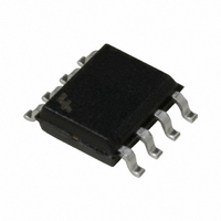
FIN1101MX Fairchild Semiconductor, FIN1101MX Datasheet - Page 3

FIN1101MX
Manufacturer Part Number
FIN1101MX
Description
IC REPEATER SGL PORT LVDS 8SOIC
Manufacturer
Fairchild Semiconductor
Type
Repeaterr
Datasheet
1.FIN1101MX.pdf
(6 pages)
Specifications of FIN1101MX
Tx/rx Type
LVDS
Delay Time
1.1ns
Capacitance - Input
2.2pF
Voltage - Supply
3 V ~ 3.6 V
Current - Supply
9.3mA
Mounting Type
Surface Mount
Package / Case
8-SOIC (3.9mm Width)
Supply Voltage (max)
3.6 V
Supply Voltage (min)
3 V
Maximum Operating Temperature
+ 150 C
Mounting Style
SMD/SMT
Interface
EIA/TIA-644-A
Minimum Operating Temperature
- 65 C
Supply Current
13.5 mA
Lead Free Status / RoHS Status
Lead free / RoHS Compliant
Available stocks
Company
Part Number
Manufacturer
Quantity
Price
t
t
t
t
t
t
f
t
t
t
t
t
t
PLHD
PHLD
TLHD
THLD
SK(P)
SK(PP)
MAX
PZHD
PZLD
PHZD
PLZD
DJ
RJ
AC Electrical Characteristics
Over supply voltage and operating temperature ranges, unless otherwise specified
Note 3: All typical values are at T
Note 4: t
direction (either LOW-to-HIGH or HIGH-to-LOW) when both devices operate with the same supply voltage, same temperature, and have identical test cir-
cuits.
Note 5: Passing criteria for maximum frequency is the output V
Note 6: Output loading is transmission line environment only; C
FIGURE 1. Differential Receiver Voltage Definitions and
Note A: All LVDS input pulses have frequency
Note B: C
Symbol
Propagation I and Transition Time Test Circuit
SK(PP)
L
includes all probe and test fixture capacitances
Differential Propagation Delay
LOW-to-HIGH
Differential Propagation Delay
HIGH-to-LOW
Differential Output Rise Time (20% to 80%)
Differential Output Fall Time (80% to 20%)
Pulse Skew |t
Part-to-Part Skew (Note 4)
Maximum Frequency (Note 5)(Note 6)
Differential Output Enable Time from Z to HIGH
Differential Output Enable Time from Z to LOW R
Differential Output Disable Time from HIGH to Z See Figure 2 and Figure 3
Differential Output Disable Time from LOW to Z
LVDS Data Jitter,
Deterministic
LVDS Clock Jitter, Random
(RMS)
is the magnitude of the difference in differential propagation delay times between identical channels of two devices switching in the same
FIGURE 3. Differential Driver Propagation Delay and Transition Time Test Circuit
PLH
- t
Parameter
A
PHL
25 C and with V
|
10MHz, t
CC
R
3.3V, V
or t
F
OD
L
is
ID
R
V
V
Duty Cycle
See Figure 3 and Figure 4
V
V
V
V
0.5 ns
200 mV and the duty cycle is 45% to 55% with all channels switching.
ID
IC
ID
IC
ID
IC
L
L
1 pF of stray test fixture capacitance.
300mV, V
100 , C
100 , C
200 mV to 450 mV,
|V
300 mV, PRBS
1.2V at 800 Mbps
300 mV
1.2 V at 400 MHz
ID
Test Conditions
|/2 to (V
3
IC
50%,
L
L
1.2V unless otherwise specified.
5 pF,
CC
5 pF,
FIGURE 2. Differential Driver DC Test Circuit
(V
2
ID
23
/2),
1,
0.75
0.75
0.29
0.29
Min
400
(Note 3)
0.40
0.40
0.01
Typ
800
1.1
1.1
2.1
2.3
1.5
1.8
2.1
85
www.fairchildsemi.com
Max
1.75
1.75
0.58
0.58
135
0.2
0.5
3.5
5
5
5
5
Units
MHz
ns
ns
ns
ns
ns
ns
ns
ns
ns
ns
ps
ps


