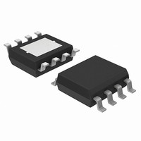
AOZ1034DI Alpha & Omega Semiconductor Inc, AOZ1034DI Datasheet - Page 7

AOZ1034DI
Manufacturer Part Number
AOZ1034DI
Description
IC BUCK SYNC ADJ 4A 8DFN
Manufacturer
Alpha & Omega Semiconductor Inc
Series
EZBuck™r
Type
Step-Down (Buck), PWM - Current Moder
Datasheet
1.AOZ1034DI.pdf
(18 pages)
Specifications of AOZ1034DI
Featured Product
The AOZ103x Family Synchronous Buck Regulator
Internal Switch(s)
Yes
Synchronous Rectifier
Yes
Number Of Outputs
1
Voltage - Output
0.8 V ~ 18 V
Current - Output
4A
Frequency - Switching
500kHz
Voltage - Input
4.5 V ~ 18 V
Operating Temperature
-40°C ~ 85°C
Mounting Type
Surface Mount
Package / Case
8-VDFN Exposed Pad
Lead Free Status / Rohs Status
Lead free / RoHS Compliant
Other names
785-1254-2
Available stocks
Company
Part Number
Manufacturer
Quantity
Price
Detailed Description
The AOZ1034 is a current-mode step down regulator
with integrated high-side PMOS switch and a low-side
NMOS switch. It operates from a 4.5V to 18V input
voltage range and supplies up to 4A of load current.
Features include enable control, Power-On Reset, input
under voltage lockout, output over voltage protection,
active high power good state, fixed internal soft-start and
thermal shut down.
The AOZ1034 comes in both a 5x4 DFN-8 and an
exposed pad SO-8 package.
Enable and Soft Start
The AOZ1034 has internal soft start feature to limit
in-rush current and ensure the output voltage ramps up
smoothly to regulation voltage. A soft start process
begins when the input voltage rises to 4.1V and voltage
on EN pin is HIGH. In soft start process, the output
voltage is ramped to regulation voltage in typically 3ms.
The 3ms soft start time is set internally.
The EN pin of the AOZ1034 is active high. Connect the
EN pin to VIN if enable function is not used. Pull it to
ground will disable the AOZ1034. Do not leave it open.
The voltage on EN pin must be above 2V to enable the
AOZ1034. When voltage on EN pin falls below 0.6V, the
AOZ1034 is disabled. If an application circuit requires the
AOZ1034 to be disabled, an open drain or open collector
circuit should be used to interface to EN pin.
Steady-State Operation
Under steady-state conditions, the converter operates
in fixed frequency and Continuous-Conduction Mode
(CCM).
The AOZ1034 integrates an internal P-MOSFET as the
high-side switch. Inductor current is sensed by amplifying
the voltage drop across the drain to source of the high
side power MOSFET. Output voltage is divided down by
the external voltage divider at the FB pin. The difference
of the FB pin voltage and reference is amplified by the
internal transconductance error amplifier. The error
voltage, which shows on the COMP pin, is compared
against the current signal, which is sum of inductor
current signal and ramp compensation signal, at PWM
comparator input. If the current signal is less than the
error voltage, the internal high-side switch is on. The
inductor current flows from the input through the inductor
to the output. When the current signal exceeds the error
voltage, the high-side switch is off. The inductor current is
Rev. 1.1 September 2010
www.aosmd.com
freewheeling through the internal low-side N-MOSFET
switch to output. The internal adaptive FET driver
guarantees no turn on overlap of both high-side and
low-side switch.
Comparing with regulators using freewheeling Schottky
diodes, the AOZ1034 uses freewheeling NMOSFET to
realize synchronous rectification. It greatly improves the
converter efficiency and reduces power loss in the
low-side switch.
The AOZ1034 uses a P-Channel MOSFET as the
high-side switch. It saves the bootstrap capacitor
normally seen in a circuit which is using an NMOS
switch. It allows 100% turn-on of the high-side switch to
achieve linear regulation mode of operation.
Switching Frequency
The AOZ1034 switching frequency is fixed and set by an
internal oscillator. The practical switching frequency
could range from 400kHz to 600kHz due to device
variation.
Light Load Mode
The AOZ1034 includes is a Pulse-Skip architecture for
Light Load operation, enabling increased efficiency
during standby. Under Heavy Loads, the controller
operates in a standard Synchronous Mode using the
high-side PMOS as control FET and low-side NMOS as
synchronous rectifier NMOS. During Light Loads, the
controller automatically switches to a Non-Synchronous
mode using the high-side PMOS as control FET and the
integrated diode as freewheeling rectifier diode.
Output Voltage Programming
Output voltage can be set by feeding back the output to
the FB pin by using a resistor divider network. In the
application circuit shown in Figure 1. The resistor divider
network includes R
by picking a fixed R
R1 with equation below.
Some standard value of R
voltage values are listed in Table 1 on the next page.
V
O
=
0.8
×
⎛
⎜
⎝
1
+
R
------ -
R
1
2
and R
1
2
value and calculating the required
⎞
⎟
⎠
1
2
, R
. Usually, a design is started
2
and most used output
AOZ1034
Page 7 of 18


