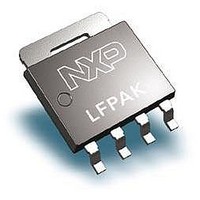
PSMN011-30YL,115 NXP Semiconductors, PSMN011-30YL,115 Datasheet - Page 8

PSMN011-30YL,115
Manufacturer Part Number
PSMN011-30YL,115
Description
MOSFET Power N-Ch 30V Trench MOS logic level FET
Manufacturer
NXP Semiconductors
Specifications of PSMN011-30YL,115
Configuration
Single
Transistor Polarity
N-Channel
Resistance Drain-source Rds (on)
10.7 mOhms
Drain-source Breakdown Voltage
30 V
Continuous Drain Current
36 A
Power Dissipation
49 W
Maximum Operating Temperature
+ 175 C
Mounting Style
SMD/SMT
Package / Case
LFPAK
Fall Time
5 ns
Gate Charge Qg
7.3 nC
Minimum Operating Temperature
- 55 C
Rise Time
8 ns
Lead Free Status / Rohs Status
Details
Other names
934064949115
NXP Semiconductors
PSMN011-30YL
Product data sheet
Fig 13. Normalized drain-source on-state resistance
Fig 15. Gate-source voltage as a function of gate
V
a
(V)
1.5
0.5
GS
10
2
1
0
8
6
4
2
0
−60
factor as a function of junction temperature
charge; typical values
T
0
j
= 25°C and I
0
6V
5
24V
D
= 45 A
60
10
120
15
V
DS
All information provided in this document is subject to legal disclaimers.
Q
003aaf442
= 15V
T
G
j
(nC)
( ° C)
03aa27
180
20
N-channel 10.7 mΩ 30 V TrenchMOS logic level FET in LFPAK
Rev. 2 — 17 May 2011
Fig 14. Gate charge waveform definitions
Fig 16. Input, output and reverse transfer capacitances
(pF)
C
10
10
10
3
2
10
as a function of drain-source voltage; typical
values
V
V
-1
GS
V
V
V
GS(pl)
DS
GS(th)
GS
= 0 V, f = 1 MHz
Q
GS1
1
I
Q
D
GS
PSMN011-30YL
Q
GS2
Q
G(tot)
Q
GD
10
© NXP B.V. 2011. All rights reserved.
V
C
DS
C
003aaa508
C
003aaf439
oss
rss
iss
(V)
10
2
8 of 14


