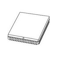
P80C592FFA NXP Semiconductors, P80C592FFA Datasheet - Page 87

P80C592FFA
Manufacturer Part Number
P80C592FFA
Description
Manufacturer
NXP Semiconductors
Datasheet
1.P80C592FFA.pdf
(108 pages)
Specifications of P80C592FFA
Cpu Family
80C
Device Core
80C51
Device Core Size
8b
Frequency (max)
16MHz
Interface Type
CAN/UART
Program Memory Type
ROMLess
Program Memory Size
Not Required
Total Internal Ram Size
512Byte
# I/os (max)
40
Number Of Timers - General Purpose
3
Operating Supply Voltage (typ)
5V
Operating Supply Voltage (max)
5.5V
Operating Supply Voltage (min)
4.5V
On-chip Adc
8-chx10-bit
Instruction Set Architecture
CISC
Operating Temp Range
-40C to 85C
Operating Temperature Classification
Industrial
Mounting
Surface Mount
Pin Count
68
Package Type
PLCC
Lead Free Status / Rohs Status
Compliant
Available stocks
Company
Part Number
Manufacturer
Quantity
Price
Company:
Part Number:
P80C592FFA
Manufacturer:
PANASONIC
Quantity:
1 200
Part Number:
P80C592FFA
Manufacturer:
PHI
Quantity:
20 000
Company:
Part Number:
P80C592FFA/00
Manufacturer:
SYSTECH
Quantity:
40
Part Number:
P80C592FFA/00
Manufacturer:
NXP/恩智浦
Quantity:
20 000
Company:
Part Number:
P80C592FFA/00,512
Manufacturer:
ON
Quantity:
300
Company:
Part Number:
P80C592FFA/00,512
Manufacturer:
NXP Semiconductors
Quantity:
10 000
Company:
Part Number:
P80C592FFA/00,518
Manufacturer:
NXP Semiconductors
Quantity:
10 000
Company:
Part Number:
P80C592FFA/00Ј¬512
Manufacturer:
NXP
Quantity:
702
Philips Semiconductors
handbook, full pagewidth
1996 Jun 27
8-bit microcontroller with on-chip CAN
are valid when
during a write
RD or WR are
during a read
from external
data memory
data memory
external data
The Port 5 input buffers have a maximum propagation delay of 300 ns.
As a result Port 5 sample time begins 300 ns before state S5 and ends
when S5 has finished.
dotted lines
only active
to external
only active
program
memory
memory
external
read or
write of
active
fetch
XTAL1
INPUT
ALE
PSEN
RD
WR
BUS
(PORT 0)
PORT 2
BUS
(PORT 0)
PORT 2
PORT
OUTPUT
PORT
INPUT
SERIAL
PORT
CLOCK
inst.
inst.
P1 P2
in
in
S1
P1 P2
address
address
A0 - A7
A0 - A7
S2
address A8 - A15
address A8 - A15
one machine cycle
P1 P2
S3
old data
Fig.30 Instruction cycle timing.
inst.
inst.
P1 P2
in
in
S4
sampling time of I/O port pins during input (including INT0 and INT1)
P1 P2
address
address
A0 - A7
A0 - A7
S5
87
address A8 - A15
P1 P2
S6
address A8 - A15 or Port 2 out
inst.
P1 P2
in
data output or data input
S1
P1 P2
address
A0 - A7
S2
address A8 - A15
one machine cycle
P1 P2
S3
new data
inst.
P1 P2
in
S4
Product specification
P1 P2
address
address
A0 - A7
A0 - A7
S5
address A8 - A15
address A8 - A15
P8xC592
P1 P2
MGA180
S6


