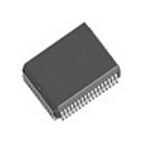
MC68150FN40 IDT, Integrated Device Technology Inc, MC68150FN40 Datasheet - Page 8

MC68150FN40
Manufacturer Part Number
MC68150FN40
Description
Manufacturer
IDT, Integrated Device Technology Inc
Datasheet
1.MC68150FN40.pdf
(40 pages)
Specifications of MC68150FN40
Operating Temperature (max)
85C
Operating Temperature (min)
-40C
Package Type
PLCC
Pin Count
68
Mounting
Surface Mount
Lead Free Status / Rohs Status
Not Compliant
Available stocks
Company
Part Number
Manufacturer
Quantity
Price
Part Number:
MC68150FN40
Manufacturer:
MOTOROLA/摩托罗拉
Quantity:
20 000
Company:
Part Number:
MC68150FN40R2
Manufacturer:
AMD
Quantity:
7
IDT™ 32-Bit to 32/16/8-Bit Dynamic READ/WRITE Bus Sizer
Freescale Timing Solutions Organization has been acquired by Integrated Device Technology, Inc
MC68150
32-Bit to 32/16/8-Bit Dynamic READ/WRITE Bus Sizer
2.4 Access Termination
by the MC68150 asserting TA during DS6. Once the TA is asserted, TA is held asserted until at least DS8. The MC68150 negates
TA asynchronously if CS is negated after DS7; an example of asynchronous termination is shown in Figure
MC68150 termination occurs when the CS is negated before DS6. See early access termination for more details.
a set-up to a DS8 rising BCLK edge. Asynchronous termination is defined as any CS negation beyond the DS8 rising BCLK edge.
In this case the TA occurs a delay after the CS negation, because it is asynchronous termination.
CS is negated, the MPU data bus goes to high impedance. If the data must be held longer than a single period, then asynchronous
TA negation is necessary.
2.5 MPU Bus Idle State
on the clock edge following TS assertion (or later) on all accesses through the MC68150. When the MPU bus is idle (between
accesses), the D(31:0) are in high impedance and TA is negated.
3. PERIPHERAL BUS OPERATION
represents half a clock period. All even states are the BCLK HIGH half of the clock period. All odd states are the BCLK LOW half
of the clock period. A clock edge is referenced by the state that follows the clock edge. All rising edges are referenced by even
number states. All falling edges are referenced by odd number states. S0 is the first state of a peripheral access. Note that the
peripheral and MPU states are distinct, though related to each other.
3.1 Initial Transfer Start
is asserted during S2. The MC68040 A(31:2) are routed past the MC68150, directly to the peripheral bus. Buffers can be used
to minimize loading on the MC68040 address bus. If the access is a write, the peripheral data bus (PD(31:16)) is driven during
S2.
are also asserted during S3. SWE is the write enable for 8-bit peripherals. The SWE is asserted for every transfer of a write access.
It indicates the data on PD(31:24) is valid and ready to be written to the 8-bit peripheral. UWE and LWE are the write enables for
16-bit peripherals. UWE indicates the data on PD(31:24) is valid and ready to be written to the 16-bit peripheral. LWE indicates
the data on PD(23:16) is valid and ready to be written to the 16-bit peripheral.
be qualified with SWE or DS for the 32-bit peripheral. An alternative is to use the UWE and LWE in conjunction with the PA1 and
PA0. If it is a 32-bit access (SIZ1 and SIZ0 = HH or LL), then apply UWE to PD(31:24), PD(15:8) and LWE to PD(23:16), PD(7:0).
If it is a 16-bit access (SIZ1 and SIZ0 = HL), then apply UWE to PD(31:24) and LWE to PD(23:16).
3.2 Initial Transfer Termination
on the falling edge of BCLK. DSACK1 and DSACK0 must remain valid for two successive falling edges of BCLK to be recognized.
If the access is a read, the PD(31:16) must be valid a set-up before the falling edge between S4 and S5. The PD(31:16) must be
held valid a hold time into S5. The DSACK1 and DSACK0 are first sampled during S2. The DSACK1 and DSACK0 are then
continuously sampled each falling edge of BCLK until the entire access is completed. This means the fastest initial transfer is two
clocks (starting S2 and ending S4).
and is the port size for the remainder of the access. Once the peripheral port size is indicated on the first transfer, all subsequent
transfers should be terminated with the same port size indication. If another port size is indicated on subsequent transfers of the
same access, the MC68150 operation is not guaranteed nor predictable. Depending upon the conditions, the MC68150 may either
MC68150
MOTOROLA
8
The final transfer on the peripheral side of the MC68150 occurs during DS5. The MC68150 access is normally terminated
For a normal access, CS is held asserted until at least DS6. TA negation is synchronous to the rising edge of DS8 if CS meets
During a read access, the data being presented to the MC68040 is held for at least one rising edge of BCLK (DS8). When
CS must remain high for one rising edge of BCLK between each access. This is guaranteed by the MC68040 if CS is asserted
The peripheral access is divided into one or more transfers. The transfers are divided into multiple states. Each state
A transfer starts off the rising edge of BCLK following the CS assertion (S2). The starting address of the transfer (PA1, PA0)
The starting data strobe (DS) is asserted during S3. If the access is a write, the starting write enables (SWE, UWE, and LWE)
A 32-bit port can generate write enables from the MC68040 normally (A1, A0, SIZ1, SIZ0 and R/W). These write enables can
Starting with S2, the MC68150 monitors the data strobe acknowledge signals (DSACK1, DSACK0) for the access termination.
Wait states are inserted into the access by maintaining DSACK1 and DSACK0 HIGH. The DSACK1 and DSACK0 are sampled
The size of the peripheral port is indicated by the DSACK1 and DSACK0. The port size must be indicated on the first transfer
Freescale Semiconductor, Inc.
For More Information On This Product,
Go to: www.freescale.com
8
High Performance Frequency
Control Products — BR1334
5
. An abnormal
NETCOM
MC68150


