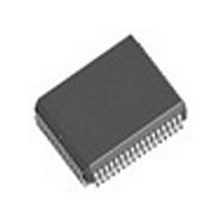
MC68150FN40 IDT, Integrated Device Technology Inc, MC68150FN40 Datasheet - Page 9

MC68150FN40
Manufacturer Part Number
MC68150FN40
Description
Manufacturer
IDT, Integrated Device Technology Inc
Datasheet
1.MC68150FN40.pdf
(40 pages)
Specifications of MC68150FN40
Operating Temperature (max)
85C
Operating Temperature (min)
-40C
Package Type
PLCC
Pin Count
68
Mounting
Surface Mount
Lead Free Status / Rohs Status
Not Compliant
Available stocks
Company
Part Number
Manufacturer
Quantity
Price
Part Number:
MC68150FN40
Manufacturer:
MOTOROLA/摩托罗拉
Quantity:
20 000
Company:
Part Number:
MC68150FN40R2
Manufacturer:
AMD
Quantity:
7
IDT™ 32-Bit to 32/16/8-Bit Dynamic READ/WRITE Bus Sizer
Freescale Timing Solutions Organization has been acquired by Integrated Device Technology, Inc
MC68150
32-Bit to 32/16/8-Bit Dynamic READ/WRITE Bus Sizer
ignore the port size change on subsequent transfers or accept the subsequent transfers as a transfer of the original port size. If
the MC68150 ignored the improper transfer, the DS is not negated. If the MC68150 accepted the improper transfer as an original
port size transfer, DS negates normally. If a different port size is indicated on subsequent transfers, the changing of DSACK1 and
DSACK0 states on subsequent transfers may or may not insert wait states into the access.
(falling edges of S3 and S5). DS is negated during S5. If the access is a write, SWE, UWE and LWE are all negated during S5.
PA1 and PA0 are held valid until S6. If the access is a write, PD(31:16) are held valid until S6.
3.3 Subsequent Access Termination
complete), then PA1 and PA0 are changed during S6. If the access is a write, PD(31:16) is changed during S6. DS, SWE, UWE
and LWE are asserted during S7. The DSACK1 and DSACK0 are sampled again for the subsequent transfer during S6.
be held valid a hold time into S9. DS, SWE, UWE and LWE are negated during S9.
S13 and S17 replacing S9 above, and S14 and S18 replacing S10. Figures
an 8-bit port, read and write respectively. Both require four sequential data transfers to complete the access.
beyond the normal access end, wait states must be inserted using DSACK1, DSACK0 = HH on the last transfer. The wait states
will delay TA assertion.
3.4 Peripheral Bus Idle State
are in high impedance. DSACK1 and DSACK0 are ignored.
3.5 Peripheral Bus Asynchronous Operation (Only for operation independant of BCLK non–680X0 processors. See AC
user to operate the peripheral bus independently of the BCLK. The synchronous operation requires close attention to the BCLK
set-up and hold times.
UWE and LWE are asserted at the same time as DS. PA1 and PA0 are valid before the DS assertion. PD(31:16) are driven and
valid before DS assertion. To avoid bus contention on the peripheral bus, the R/W from the MPU can be used.
asserted on one falling edge, the asynchronous skew specification ensures that the other DSACK signal is valid before the next
falling edge. Because the DSACK signals can be changing on a falling BCLK edge, an additional wait state may be incurred.
DSACK1 and DSACK0 can be negated when DS is negated.
LWE and SWE are negated.
High Performance Frequency
Control Products — BR1334
When a valid DSACK1 and DSACK0 state has been held for two consecutive falling edges of BCLK, the intial transfer is ended
If additional transfers are required to complete an access (e.g. a long word access to a byte port requires four transfers to
If the access is a read, the PD(31:16) must be valid a set-up before the falling edge between S8 and S9. The PD(31:16) must
Subsequent transfers continue in the same manner with S10 and S14 replacing S6 above, S11 and S15 replacing S7 above,
On a write, the PD(31:16) bus goes into high impedance when TA asserts (DS6). To hold the data valid on the PD(31:16) bus
The MC68150 enters an idle state on the peripheral bus on the rising edge of BCLK after the last transfer is terminated.
When the peripheral bus is idle, DS, UWE, LWE and SWE are all negated. PA1 and PA0 are driven, but undefined. PD(31:16)
The MC68150 peripheral bus has both asynchronous and sychronous operations. The asynchronous operation allows the
An asynchronous transfer on the MC68150 begins with the assertion of DS by the MC68150. If the access is a write, SWE,
The DSACK1 and DSACK0 assertions must be within the asynchronous skew specification. If one of the DSACK signals is
If the access is a write, the UWE, LWE and SWE negate at the same time as DS. PD(31:16) change state after the DS, UWE,
If the access is a read, PD(31:0) is valid after DSACK1 and DSACK0 are asserted and held until DS is negated.
Table 3. DSACK1 AND DSACK0 DECODE LOGIC
CS
H
L
L
L
L
Freescale Semiconductor, Inc.
For More Information On This Product,
DSACK1
X
H
H
L
L
Specifications 22–34 in lieu of specs 1–21)
Go to: www.freescale.com
DSACK0
X
H
H
L
L
9
No Access
Complete 32-Bit Access
Complete 16-Bit Access
Complete 8-Bit Access
Insert Wait States
13
and
14
are examples of 32-bit ‘040 access from/to
MC68150
MOTOROLA
NETCOM
9
MC68150


