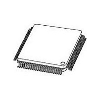
PXAH40KFBE NXP Semiconductors, PXAH40KFBE Datasheet - Page 29

PXAH40KFBE
Manufacturer Part Number
PXAH40KFBE
Description
Manufacturer
NXP Semiconductors
Datasheet
1.PXAH40KFBE.pdf
(42 pages)
Specifications of PXAH40KFBE
Cpu Family
XA
Device Core
80C51
Device Core Size
16b
Frequency (max)
30MHz
Interface Type
USART
Program Memory Type
ROMLess
Program Memory Size
Not Required
# I/os (max)
32
Number Of Timers - General Purpose
2
Operating Supply Voltage (typ)
3.3/5V
Operating Supply Voltage (max)
5.5V
Operating Supply Voltage (min)
2.97V
Instruction Set Architecture
CISC
Operating Temp Range
-40C to 85C
Operating Temperature Classification
Industrial
Mounting
Surface Mount
Pin Count
100
Package Type
LQFP
Lead Free Status / Rohs Status
Compliant
Available stocks
Company
Part Number
Manufacturer
Quantity
Price
Company:
Part Number:
PXAH40KFBE
Manufacturer:
TriQuint
Quantity:
1 200
Part Number:
PXAH40KFBE
Manufacturer:
NXP/恩智浦
Quantity:
20 000
Company:
Part Number:
PXAH40KFBE,557
Manufacturer:
NXP Semiconductors
Quantity:
10 000
1. See notes after the 3.3 V AC Timing Table
Philips Semiconductors
PRELIMINARY AC ELECTRICAL CHARACTERISTICS (5.0 V +/–10%)
V
NOTE:
1999 Sep 24
DD
Symbol
Symbol
t
t
t
t
t
t
t
t
t
t
t
t
t
t
t
t
Single-chip 16-bit microcontroller
t
t
t
CODH
CPWH
CHCX
CHAH
CHSH
CPWL
AHDR
OHDE
CHDV
SHAH
SHDH
CLCX
CLCH
CHCL
CHAV
CHSL
DVSL
CLRL
AVSL
t
t
t
t
t
F
DIS
DIH
WS
WH
t
RP
= 5.0 V +/– 10%; T
C
C
7, 8, 10, 11, 12, 14, 15,
7, 8, 10, 14, 15, 17, 18
11, 12, 17, 18, 19, 20
8, 10, 11, 14, 18
17, 18, 19
Fig re
Figure
11, 19
16, 20
7, 14
9, 13
9, 16
9, 16
amb
23
23
23
23
23
All
All
All
All
All
24
22
21
25
25
= –40 C to +85 C (industrial)
System Clock Frequency
System Clock Period = 1/FC
XTALIN High Time
XTALIN Low Time
XTALIN Rise Time
XTALIN Fall Time
Address Valid to Strobe low
Address hold after ClkOut rising edge
Delay from ClkOut rising edge to address valid
Delay from ClkOut rising edge to Strobe High
Delay from ClkOut rising edge to Strobe Low
ClkOut Duty Cycle High (into 40 pF max.)
CAS Pulse Width High
CAS Pulse Width Low
RAS precharge time, thus minimum RAS high time
Address hold (A19 – A1 only, not A0) after CS, BLE, BHE rise at
end of Generic Data Read Cycle (not code fetch)
Data In Valid setup to ClkOut rising edge
Data In Valid hold after ClkOut rising edge
OE high to XA Data Bus Driver Enable
Clock High to Data Valid
Data Valid prior to Strobe Low
Minimum Address Hold Time after strobe goes inactive
Data hold after strobes (CS and BHE/BLE) high
CAS low to RAS low
WAIT setup (stable high or low) to ClkOut rising edge
WAIT hold (stable high or low) after ClkOut rising edge
Data Read and Instruction Fetch Cycles
Generic Data Read Only
All DRAM Cycles
Write Cycles
All Cycles
Wait Input
Parameter
Parameter
Refresh
29
9
2
9
9
8
(n * t
t
t
t
t
t
t
t
t
t
t
t
t
CHCX
33.33
C
C
C
C
C
C
C
C
C
C
C
Min
C
* 0.5
* 0.4
25
20
– 21
– 12
– 10
– 12
– 14
– 23
– 25
– 25
– 15
0
–
–
1
–
1
1
0
–
0
) – 16
–7
Limits
8
Preliminary specification
t
CHCX
Max
30
25
21
19
25
–
–
–
5
5
–
–
–
–
–
–
–
–
–
–
–
–
–
–
–
XA-H4
+3
MHz
Unit
Unit
ns
ns
ns
ns
ns
ns
ns
ns
ns
ns
ns
ns
ns
ns
ns
ns
ns
ns
ns
ns
ns
ns
ns
ns
ns


