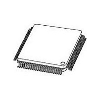
PXAH40KFBE NXP Semiconductors, PXAH40KFBE Datasheet - Page 9

PXAH40KFBE
Manufacturer Part Number
PXAH40KFBE
Description
Manufacturer
NXP Semiconductors
Datasheet
1.PXAH40KFBE.pdf
(42 pages)
Specifications of PXAH40KFBE
Cpu Family
XA
Device Core
80C51
Device Core Size
16b
Frequency (max)
30MHz
Interface Type
USART
Program Memory Type
ROMLess
Program Memory Size
Not Required
# I/os (max)
32
Number Of Timers - General Purpose
2
Operating Supply Voltage (typ)
3.3/5V
Operating Supply Voltage (max)
5.5V
Operating Supply Voltage (min)
2.97V
Instruction Set Architecture
CISC
Operating Temp Range
-40C to 85C
Operating Temperature Classification
Industrial
Mounting
Surface Mount
Pin Count
100
Package Type
LQFP
Lead Free Status / Rohs Status
Compliant
Available stocks
Company
Part Number
Manufacturer
Quantity
Price
Company:
Part Number:
PXAH40KFBE
Manufacturer:
TriQuint
Quantity:
1 200
Part Number:
PXAH40KFBE
Manufacturer:
NXP/恩智浦
Quantity:
20 000
Company:
Part Number:
PXAH40KFBE,557
Manufacturer:
NXP Semiconductors
Quantity:
10 000
1. See XA-H4 User Guide, “Pins Chapter,” for how to program selection of pin functions.
2. RTClk input is usually used for Rx Clock if an external clock is needed, but can be used for either Rx or Tx or both. TRClk is usually used for
Philips Semiconductors
NOTES:
1999 Sep 24
Mnemonic
CD1_Int2
Single-chip 16-bit microcontroller
Tx Clock, but can be used for Rx or Tx or both.
GPOut
RxD0
TxD0
P1.0
P1.1
P1.2
P1.3
P1.4
P1.5
P1.6
P1.7
P2.0
P2.1
P2.2
P2.3
P2.4
P2.5
P2.6
P2.7
P3.0
P3.1
P3.2
P3.3
P3.4
P3.5
P3.6
P3.7
Int0
Pin No.
Lqfp
96
97
98
68
69
70
71
72
73
74
75
80
81
82
83
84
85
86
87
56
57
58
63
64
65
66
67
78
79
Type
I/O
I/O
I/O
I/O
I/O
I/O
I/O
I/O
I/O
I/O
I/O
I/O
I/O
I/O
I/O
I/O
I/O
I/O
I/O
I/O
I/O
I/O
I/O
I/O
I/O
I/O
O
O
I
TxD0: Transmit data for USART0.
RxD0: Receive data for USART0.
GPOut – General Purpose Output Bar: Similar to GPIO, but Push/Pull and inverted output only.
WARNING: This output is inverted. The polarity of the pin is the opposite of the bit that drives it
(GPOut[7])
P1.0_RxD2: Port 1 Bit 0, or USART2 RxD input
P1.1_TxD2: Port 1 Bit 1, or USART2 TxD output
P1.2_RTClk2: Port 1 Bit 2, or USART2 RT Clock input
P1.3_TRClk2: Port 1 Bit 3, or USART2 TR Clock input
P1.4_CD2: Port 1 Bit 4, or USART2 Carrier Detect input
P1.5_CTS2: Port 1 Bit 5, or USART2 Clear To Send input
P1.6_RTS2: Port 1 Bit 6, or USART2 Request To Send output
P1.7_BRG2_Sync2: Port 1 Bit 7, or USART2 Sync input or output, or BRG output, or TxClk
output (see USART clk diagrams in the user manual . )
P2.0_RxD3: Port 2 Bit 0, or USART3 Rx Data input
P2.1_TxD3: Port 2 Bit 1, or USART3 Tx Data output
P2.2_RTClk3: Port 2 Bit 2, or USART3 RT Clock input
P2.3_ComClk_TRClk3: Port 2 Bit 3, or USART3 TR Clock input
P2.4_CD3: Port 2 Bit 4, or USART3 Carrier Detect input
P2.5_CTS3: Port 2 Bit 5, or USART3 Clear To Send input
P2.6_RTS3: Port 2 Bit 6, or USART3 Request To Send output
P2.7_Sync3_BRG3: Port 2 Bit 7, or USART3 Sync input or output, or BRG output, or TxClk
output (see USART clock diagrams in the user manual . )
P3.0_CS4_RAS4_RTClk1: Port 3 Bit 0, or CS4 or RAS 4 output, or USART1 RT Clock input
Active low chip selects CS1 through CS5 come out of reset disabled. They can be programmed to
function as normal chip selects, or as RAS strobes to DRAM. CS2 through CS5 are not used with
the “SWAP” operation (see the “Memory Controller” chapter in the XA-H4 User Manual .) They are
mappable to any region of the 16 MB address space.
P3.1_CS5_RTS1: Port 3 Bit 1, or CS5 output, or USART1 Request To Send output
Active low chip selects CS1 through CS5 come out of reset disabled. They can be programmed to
function as normal chip selects, or as RAS strobes to DRAM. CS2 through CS5 are not used with
the “SWAP” operation (see the “Memory Controller” chapter in the XA-H4 User Manual .) They are
mappable to any region of the 16 MB address space.
P3.2_Timer0_ResetOut: Port 3 Bit 2, or Timer0 input or output, or ResetOut output.
ResetOut: If the ResetOut function is selected, this pin outputs a low whenever the XA-H4
processor is reset by an internal source (Watchdog Reset or the RESET instruction.)
WARNING: Unlike the other 31 GPIO pins, during power up reset, this pin can output a strongly
driven low pulse. The duration of this low pulse ranges from 0 ns to 258 system clocks, starting at
the time that V
When used as GPIO, this pin can be driven low by software without resetting the XA-H4.
P3.3_Timer1_BRG1_Sync1: Port 3 Bit 3, or Timer1 input or output, or USART1 BRG output, or
USART1 Sync input or output.
P3.4_CTS1: Port 3 Bit 4, or USART1 Clear To Send input
P3.5_RxD1: Port 3 Bit 5, or USART1 Receive Data input
P3.6_TxD1: Port 3 Bit 6, or USART1 Transmit Data output
P3.7_Int1_TRClk1: Port 3 Bit 7, or External Interrupt 1 input, or USART1 TR Clock input
CD1_Int2: USART1 Carrier Detect, or External Interrupt 2
External Interrupt 0
CC
is valid. The state of the ResetIn pin does not affect this pulse.
9
Name and Function
Preliminary specification
XA-H4
Note
See
2
2
2
2
2
2


