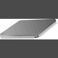
PC87393VJG National Semiconductor, PC87393VJG Datasheet - Page 107

PC87393VJG
Manufacturer Part Number
PC87393VJG
Description
IC, SUPER I/O DEVICE, TQFP-100
Manufacturer
National Semiconductor
Specifications of PC87393VJG
Data Rate
2Mbps
Supply Voltage Range
3V to 3.6V
Logic Case Style
TQFP
No. Of Pins
100
Operating Temperature Range
0°C to +70°C
Termination Type
SMD
Transceiver Type
Interface
Rohs Compliant
No
Available stocks
Company
Part Number
Manufacturer
Quantity
Price
Part Number:
PC87393VJG
Manufacturer:
NS/国半
Quantity:
20 000
7.0 X-Bus Extension
The X-Bus interface outputs the address in one of two modes:
X-Bus access timing is driven by an internal version of the LPC clock (i.e., it has the same frequency but may have some
phase delay), referred to in this section simply as "the clock". The transactions are described in reference to the clock, and
the AC specifications are relative to it. This provides an easy way for calculating the timing for the system design. However,
the system interface is optimized for an asynchronous interface. For hints on how to use it, refer to the usage hints in Section
7.5.
7.3.1
The PC8739x has two chip select signals, XCS1-0, to indicate X-Bus accesses. The PC8739x X-Bus functional block en-
ables flexible association of these chip selects with I/O and memory address ranges in the LPC address space. The Chip
Select Mapping field of the X-Bus Zone Configuration registers defines to which of the decoded address ranges the respec-
tive XCS signal responds. In addition, the X-Bus Configuration register enables specifying the access time for the respective
select signal via bits that control the fixed wait cycles and variable wait cycles, using the XRDY input.
If the chip select signal setting results in a conflict in which both selects are configured for the same transaction, XCS0 has
priority. XCS1 remains inactive and its Configuration register setting is ignored. For zones that are not associated with one
of the chip select signals, the X-Bus does not respond to LPC transactions.
7.3.2
The BIOS memory on the LPC bus can occupy one of three regions in the memory space (specified in Table 29 and Table
31). Address translation between the LPC bus address and the X-Bus is performed as follows:
I/O Transactions. The 16-bit address of the LPC bus is padded with zeroes (bits 16 through 27) to create the 28-bit input
address to the X-Bus functional block.
Memory Transactions. The 32-bit address received from the LPC bus is used to decode the different zones described in
Section 2.19. The address is then translated to the X-Bus address using the following rules:
Normal Address mode - A pin is assigned for each address line, and a non-multiplexed address data bus is used.
Latched Address mode - The number of pins used for outputting the address is reduced. The address lines are mul-
tiplexed with the data bus. External latches should be used to enable the memory or I/O device access to the multi-
plexed address signals. When the memory configuration uses more than 1 Mbyte of memory, this mode must be
used to generate address signals 20 through 27.
User-Defined Zone (UDZ) and 386 Mode-Compatible BIOS Range (LPC or LPC-FWH) - The 28 least significant bits
of the LPC address are used as the X-Bus input address. Figure 22 illustrates the mapping for this zone. (Note: See
Section 2.8.1 for the way addresses are built for FWH transactions.)
Legacy and Extended Legacy BIOS Range - The 17 least significant bits (A16-0) of the LPC address are routed as
the 17 least significant signals address lines of the X-Bus (XA16-0). The upper 11 X-Bus address lines are driven to
1. This shifts the addresses to the end of the X-Bus memory space (see Figure 23).
Programmable I/O Range Chip Select
LPC and FWH Address to X-Bus Address Translation
Figure 22. LPC to X-Bus Address Translation: 386 Mode-Compatible BIOS Range
FFFFFFFFh
FFC00000h
00000000h
(Continued)
LPC Bus Address
107
X-Bus Address
xFC00000h
xFFFFFFFh
www.national.com


