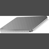
PC87393VJG National Semiconductor, PC87393VJG Datasheet - Page 57

PC87393VJG
Manufacturer Part Number
PC87393VJG
Description
IC, SUPER I/O DEVICE, TQFP-100
Manufacturer
National Semiconductor
Specifications of PC87393VJG
Data Rate
2Mbps
Supply Voltage Range
3V to 3.6V
Logic Case Style
TQFP
No. Of Pins
100
Operating Temperature Range
0°C to +70°C
Termination Type
SMD
Transceiver Type
Interface
Rohs Compliant
No
Available stocks
Company
Part Number
Manufacturer
Quantity
Price
Part Number:
PC87393VJG
Manufacturer:
NS/国半
Quantity:
20 000
- Current page: 57 of 148
- Download datasheet (2Mb)
2.0 Device Architecture and Configuration
2.15.3 Logical Device 7 (GPIO) Configuration
Table 24 lists the configuration registers which affect the GPIO. Only the last three registers (F0h - F2h) are described here.
See Sections 2.2.3 and 2.2.4 for a detailed description of the others.
Figure 6 shows the organization of these registers.
Index
30h
60h
61h
70h
71h
74h
75h
F0h
F1h
F2h
Configuration Register
Routing Register
GPIO Pin Event
(Index F2h)
(Index F1h)
Activate. See also bit 7 of the SIOCF1 register.
Base Address MSB register
Base Address LSB register. Bits 3-0 (for A3-0) are read only, 0000b.
Interrupt Number and Wake-Up on IRQ Enable register
Interrupt Type. Bit 1 is read/write. Other bits are read only.
Report no DMA assignment
Report no DMA assignment
GPIO Pin Select register
GPIO Pin Configuration register
GPIO Pin Event Routing register
GPIO Pin
Configuration Register or Action
Figure 6. Organization of GPIO Pin Registers
Port Select
GPIO Pin Select Register
Table 24. GPIO Configuration Register
(Index F0h)
Port 0
Port 0
Port 1
Port 3
Pin Select
57
(Continued)
Pin 0
Pin 0
Pin 7
Pin 7
Port 0, Pin 0
Port 0, Pin 0
Port 0, Pin 7
Port 0, Pin 7
Port 1, Pin 0
Port 1, Pin 0
Configuration Registers
Port 2, Pin 0
Event Routing
Port 3, Pin 0
Registers
Type
R/W
R/W
R/W
R/W
R/W
R/W
R/W
R/W
RO
RO
Reset
00h
00h
00h
00h
03h
04h
04h
00h
44h
01h
www.national.com
Related parts for PC87393VJG
Image
Part Number
Description
Manufacturer
Datasheet
Request
R
Part Number:
Description:
National Semiconductor [8-Bit D/A Converter]
Manufacturer:
National Semiconductor
Datasheet:
Part Number:
Description:
National Semiconductor [Media Coprocessor]
Manufacturer:
National Semiconductor
Datasheet:
Part Number:
Description:
Digitally Controlled Tone and Volume Circuit with Stereo Audio Power Amplifier, Microphone Preamp Stage and National 3D Sound
Manufacturer:
National Semiconductor
Datasheet:
Part Number:
Description:
Digitally Controlled Tone and Volume Circuit with Stereo Audio Power Amplifier, Microphone Preamp Stage and National 3D Sound
Manufacturer:
National Semiconductor
Datasheet:
Part Number:
Description:
AC97 Rev 2 Codec with Sample Rate Conversion and National 3D Sound
Manufacturer:
National Semiconductor
Part Number:
Description:
Manufacturer:
National Semiconductor
Datasheet:
Part Number:
Description:
Manufacturer:
National Semiconductor
Datasheet:
Part Number:
Description:
General Purpose, Low Voltage, Low Power, Rail-to-Rail Output Operational Amplifiers
Manufacturer:
National Semiconductor
Datasheet:
Part Number:
Description:
8-bit 20 MSPS flash A/D converter.
Manufacturer:
National Semiconductor
Datasheet:
Part Number:
Description:
Low Noise Quad Operational Amplifier
Manufacturer:
National Semiconductor
Datasheet:
Part Number:
Description:
Quad Differential Line Receivers
Manufacturer:
National Semiconductor
Datasheet:
Part Number:
Description:
Quad High Speed Trapezoidal? Bus Transceiver
Manufacturer:
National Semiconductor
Datasheet:
Part Number:
Description:
Dual Line Receiver
Manufacturer:
National Semiconductor
Datasheet:
Part Number:
Description:
TTL to 10k ECL Level Translator with Latch
Manufacturer:
National Semiconductor
Datasheet:


