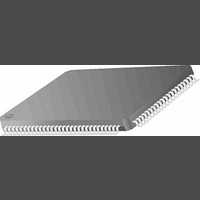
PC87393VJG National Semiconductor, PC87393VJG Datasheet - Page 35

PC87393VJG
Manufacturer Part Number
PC87393VJG
Description
IC, SUPER I/O DEVICE, TQFP-100
Manufacturer
National Semiconductor
Specifications of PC87393VJG
Data Rate
2Mbps
Supply Voltage Range
3V to 3.6V
Logic Case Style
TQFP
No. Of Pins
100
Operating Temperature Range
0°C to +70°C
Termination Type
SMD
Transceiver Type
Interface
Rohs Compliant
No
Available stocks
Company
Part Number
Manufacturer
Quantity
Price
Part Number:
PC87393VJG
Manufacturer:
NS/国半
Quantity:
20 000
- Current page: 35 of 148
- Download datasheet (2Mb)
2.0 Device Architecture and Configuration
The Parallel Port pins function as an FDD interface for either drive 1 or drive 3. See Figure 5 for the internal routing between
the PPM and FDC, and the Parallel Port and FDC pin-sets when PPM mode is active. The FDC output signals are driven
simultaneously both on the normal FDC pins and on the corresponding Parallel Port pins. The FDC inputs are received from
the FDC pins when either drive 0 or drive 2 is selected, and from the corresponding Parallel Port pins when either drive 1 or
drive 3 is selected.
The Parallel Port output signals are isolated from the Parallel Port pins. The Parallel Port input signals, as reflected by the
STR register, assume one of two possible values ([BUSY, PE, SLCT, ACK] = 1001 or 1111), indicating that nothing is con-
nected to the Parallel Port. The default values are controlled by bit 2 of the Parallel Port Configuration register (see Section
2.12.3 for details).
PPM is in power save mode when PPM is active and the PPM power save mode bit is enabled.See Section 2.6.1 for details.
2.6.1
PPM power save mode helps avoid the additional power consumption associated with driving two sets of FDD outputs by
limiting the activity to the selected drive only. PPM power save mode is enabled by bit 2 of the SIOCF5 register, and is in
effect only when the PPM is active. Assuming that the internal FDD (on the normal FDC pins) is drive 0, while the external
FDD (on the Parallel Port pins) is drive 1, the outputs of the non-selected drive do not toggle, but rather are frozen at their
inactive levels. Table 14 shows the behavior of the FDC outputs on both the FDC and Parallel Port pins when the PPM is
active and PPM power save mode is enabled.
PPM Active
and bit 7 of SIOCF5 is ’0’ (PNF=0)
PPM Power Save Mode
Parallel
FDC
Port
Signal
DR0
0
1
1
PPM in Power Save Mode
PPM in Power Save Mode
Table 14. FDC Output Status in PPM Power Save Mode
and Drive 1 Selected
and Drive 0 Selected
PPM Power Save
at Inactive Levels
at Inactive Levels
Signal
Outputs Frozen
Outputs Frozen
DR1
1
0
1
Figure 5. PPM Routing
Functional
Frozen at inactive levels
Functional
0
1
FDC Pins
35
(Continued)
Parallel Port Input Values
Drive 1 or 3 Selected
Default “Non-Connect”
PPM Active and
FDC Outputs
0
0
1
1
FDC Outputs
Frozen at inactive levels
Functional
Functional
Parallel Port
Outputs
FDC Outputs
Parallel Port Pins
FDC Inputs
Parallel Port Inputs
FDC Inputs
FDC Pins
Parallel Port Pins
www.national.com
Related parts for PC87393VJG
Image
Part Number
Description
Manufacturer
Datasheet
Request
R
Part Number:
Description:
National Semiconductor [8-Bit D/A Converter]
Manufacturer:
National Semiconductor
Datasheet:
Part Number:
Description:
National Semiconductor [Media Coprocessor]
Manufacturer:
National Semiconductor
Datasheet:
Part Number:
Description:
Digitally Controlled Tone and Volume Circuit with Stereo Audio Power Amplifier, Microphone Preamp Stage and National 3D Sound
Manufacturer:
National Semiconductor
Datasheet:
Part Number:
Description:
Digitally Controlled Tone and Volume Circuit with Stereo Audio Power Amplifier, Microphone Preamp Stage and National 3D Sound
Manufacturer:
National Semiconductor
Datasheet:
Part Number:
Description:
AC97 Rev 2 Codec with Sample Rate Conversion and National 3D Sound
Manufacturer:
National Semiconductor
Part Number:
Description:
Manufacturer:
National Semiconductor
Datasheet:
Part Number:
Description:
Manufacturer:
National Semiconductor
Datasheet:
Part Number:
Description:
General Purpose, Low Voltage, Low Power, Rail-to-Rail Output Operational Amplifiers
Manufacturer:
National Semiconductor
Datasheet:
Part Number:
Description:
8-bit 20 MSPS flash A/D converter.
Manufacturer:
National Semiconductor
Datasheet:
Part Number:
Description:
Low Noise Quad Operational Amplifier
Manufacturer:
National Semiconductor
Datasheet:
Part Number:
Description:
Quad Differential Line Receivers
Manufacturer:
National Semiconductor
Datasheet:
Part Number:
Description:
Quad High Speed Trapezoidal? Bus Transceiver
Manufacturer:
National Semiconductor
Datasheet:
Part Number:
Description:
Dual Line Receiver
Manufacturer:
National Semiconductor
Datasheet:
Part Number:
Description:
TTL to 10k ECL Level Translator with Latch
Manufacturer:
National Semiconductor
Datasheet:


