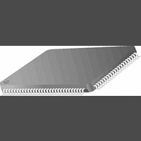
PC87393VJG National Semiconductor, PC87393VJG Datasheet - Page 26

PC87393VJG
Manufacturer Part Number
PC87393VJG
Description
IC, SUPER I/O DEVICE, TQFP-100
Manufacturer
National Semiconductor
Specifications of PC87393VJG
Data Rate
2Mbps
Supply Voltage Range
3V to 3.6V
Logic Case Style
TQFP
No. Of Pins
100
Operating Temperature Range
0°C to +70°C
Termination Type
SMD
Transceiver Type
Interface
Rohs Compliant
No
Available stocks
Company
Part Number
Manufacturer
Quantity
Price
Part Number:
PC87393VJG
Manufacturer:
NS/国半
Quantity:
20 000
2.0 Device Architecture and Configuration
The PC8739x SuperI/O device comprises a collection of legacy and proprietary functional blocks. Each functional block is
described in a separate chapter in this document. However, some parameters in the implementation of each functional block
may vary per SuperI/O device. This chapter describes the PC8739x structure and provides all logical device specific infor-
mation, including special implementation of generic blocks, system interface and device configuration.
2.1 OVERVIEW
The PC8739x consists of 9 logical devices, the host interface, and a central set of configuration registers, all built around a
central, internal bus. The internal bus is similar to an 8-bit ISA bus protocol. See Figure 1, which illustrates the blocks and
related logic.
The system interface serves as a bridge between the external LPC interface and the internal bus. It supports 8-bit Read and
Write transactions for I/O, memory, DMA, and FWH, as defined in Intel’s LPC Interface Specification, Revision 1.01 .
The central configuration register set is ACPI compliant and supports a PnP configuration. The configuration registers are struc-
tured as a subset of the Plug and Play Standard registers, defined in Appendix A of the Plug and Play ISA Specification, Re-
vision 1.0a by Intel and Microsoft. All system resources assigned to the functional blocks (I/O address space, DMA channels
and IRQ lines) are configured in, and managed by, the central configuration register set. In addition, some function-specific
parameters are configurable through the configuration registers and distributed to the functional blocks through special control
signals.
2.2 CONFIGURATION STRUCTURE AND ACCESS
The configuration structure is comprised of a set of banked registers which are accessed via a pair of specialized registers.
2.2.1
Access to the SuperI/O configuration registers is via an Index-Data register pair, using only two system I/O byte locations.
The base address of this register pair is determined during reset, according to the state of the hardware strapping option on
the BADDR pin. Table 5 shows the selected base addresses as a function of BADDR.
The Index register is an 8-bit read/write register located at the selected base address (Base+0). It is used as a pointer to the
configuration register file, and holds the index of the configuration register that is currently accessible via the Data register.
Reading the Index register returns the last value written to it (or the default of 00h after reset).
The Data register is an 8-bit register (Base+1) used as a data path to any configuration register. Accessing the Data register
actually accesses the configuration register that is currently pointed to by the Index register.
The Index-Data Register Pair
BADDR
Table 5. BADDR Strapping Options
0
1
Index Register
2Eh
4Eh
26
I/O Address
Data Register
2Fh
4Fh
www.national.com


