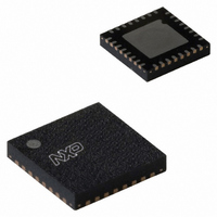
SC16C850IBS,151 NXP Semiconductors, SC16C850IBS,151 Datasheet - Page 39

SC16C850IBS,151
Manufacturer Part Number
SC16C850IBS,151
Description
IC UART SGL-CH 3.3V 32-HVQFN
Manufacturer
NXP Semiconductors
Datasheet
1.SC16C850IBS151.pdf
(55 pages)
Specifications of SC16C850IBS,151
Package / Case
32-VFQFN Exposed Pad
Features
Programmable
Number Of Channels
1, UART
Fifo's
128 Byte
Protocol
RS485
Voltage - Supply
2.5 V ~ 3.3 V
With Auto Flow Control
Yes
With Irda Encoder/decoder
Yes
With False Start Bit Detection
Yes
With Modem Control
Yes
With Cmos
Yes
Mounting Type
Surface Mount
Data Rate
5 Mbps
Supply Voltage (max)
3.3 V
Supply Voltage (min)
2.5 V
Supply Current
2 mA
Maximum Operating Temperature
+ 85 C
Minimum Operating Temperature
- 40 C
Mounting Style
SMD/SMT
Lead Free Status / RoHS Status
Lead free / RoHS Compliant
Lead Free Status / RoHS Status
Lead free / RoHS Compliant, Lead free / RoHS Compliant
Other names
568-4778
935283103151
935283103151
NXP Semiconductors
10. Dynamic characteristics
Table 37.
T
[1]
[2]
[3]
[4]
SC16C850
Product data sheet
Symbol
t
t
t
f
t
t
t
t
t
t
t
t
t
t
t
t
t
t
t
t
t
t
t
t
t
t
N
WH
WL
w(clk)
XTAL1
su(A)
h(A)
d(CS-IOR)
w(IOR)
h(IOR-CS)
d(IOR)
d(IOR-Q)
dis(IOR-QZ)
d(CSL-IOWL)
w(IOW)
h(IOW-CS)
d(IOW)
su(D-IOWH)
h(IOWH-D)
d(IOW-Q)
d(modem-INT)
d(IOR-INTL)
d(stop-INT)
d(start-INT)
d(IOW-TX)
d(IOW-INTL)
w(RESET)
amb
Applies to external clock, crystal oscillator max 24 MHz.
Maximum frequency =
10 % of the data bus output voltage level.
RCLK is an internal signal derived from Divisor Latch LSB (DLL) and Divisor Latch MSB (DLM) divisor latches.
=
−
40
°
Dynamic characteristics - Intel or 16 mode
C to +85
Parameter
pulse width HIGH
pulse width LOW
clock pulse width
frequency on pin XTAL1
address set-up time
address hold time
delay time from CS to IOR
IOR pulse width time
hold time from IOR to chip select
IOR delay time
delay time from IOR to data output
disable time from IOR to
high-impedance data output
delay time from CS LOW to
IOW LOW
IOW pulse width time
hold time from IOW to CS
IOW delay time
set-up time from data input to
IOW HIGH
data input hold time after IOW HIGH
delay time from IOW to data output
delay time from modem to INT
delay time from IOR to INT LOW
delay time from stop to INT
delay time from start to INT
delay time from IOW to TX
delay time from IOW to INT LOW
pulse width on pin RESET
baud rate divisor
°
C; tolerance of V
-------------- -
t
w clk
(
1
)
DD
[3]
All information provided in this document is subject to legal disclaimers.
±
10 %; unless otherwise specified.
2.5 to 3.3 V UART with 128-byte FIFOs and IrDA encoder/decoder
Rev. 2 — 11 November 2010
25 pF load
25 pF load
Conditions
25 pF load
25 pF load
25 pF load
25 pF load
25 pF load
25 pF load
25 pF load
[1][2]
[4]
[4]
[4]
8T
12.5
Min
10
10
10
35
10
10
15
15
10
10
10
RCLK
6
6
0
0
1
V
-
-
-
-
-
-
-
-
-
DD
= 2.5 V
24T
(2
1T
1T
Max
16
80
35
17
40
35
35
55
RCLK
RCLK
-
-
-
-
-
-
-
-
-
-
-
-
-
-
-
-
RCLK
− 1)
8T
12.5
Min
26
10
20
20
10
RCLK
SC16C850
6
6
5
5
5
0
5
0
5
5
1
V
-
-
-
-
-
-
-
-
-
DD
© NXP B.V. 2010. All rights reserved.
= 3.3 V
24T
(2
1T
1T
Max
16
80
26
15
33
24
24
45
RCLK
RCLK
-
-
-
-
-
-
-
-
-
-
-
-
-
-
-
-
RCLK
− 1)
39 of 55
Unit
ns
ns
ns
MHz
ns
ns
ns
ns
ns
ns
ns
ns
ns
ns
ns
ns
ns
ns
ns
ns
ns
s
s
s
ns
ns


