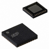
SC16C850IBS,151 NXP Semiconductors, SC16C850IBS,151 Datasheet - Page 8

SC16C850IBS,151
Manufacturer Part Number
SC16C850IBS,151
Description
IC UART SGL-CH 3.3V 32-HVQFN
Manufacturer
NXP Semiconductors
Datasheet
1.SC16C850IBS151.pdf
(55 pages)
Specifications of SC16C850IBS,151
Package / Case
32-VFQFN Exposed Pad
Features
Programmable
Number Of Channels
1, UART
Fifo's
128 Byte
Protocol
RS485
Voltage - Supply
2.5 V ~ 3.3 V
With Auto Flow Control
Yes
With Irda Encoder/decoder
Yes
With False Start Bit Detection
Yes
With Modem Control
Yes
With Cmos
Yes
Mounting Type
Surface Mount
Data Rate
5 Mbps
Supply Voltage (max)
3.3 V
Supply Voltage (min)
2.5 V
Supply Current
2 mA
Maximum Operating Temperature
+ 85 C
Minimum Operating Temperature
- 40 C
Mounting Style
SMD/SMT
Lead Free Status / RoHS Status
Lead free / RoHS Compliant
Lead Free Status / RoHS Status
Lead free / RoHS Compliant, Lead free / RoHS Compliant
Other names
568-4778
935283103151
935283103151
NXP Semiconductors
Table 2.
[1]
SC16C850
Product data sheet
Symbol
RTS
RX
TX
V
V
XTAL1
XTAL2
DD
SS
HVQFN32 package die supply ground is connected to both V
ground for proper device operation. For enhanced thermal, electrical, and board level performance, the exposed pad needs to be
soldered to the board using a corresponding thermal pad on the board and for proper heat conduction through the board, thermal vias
need to be incorporated in the PCB in the thermal pad region.
Pin description
C5
Pin
TFBGA36 HVQFN32
D2
C6
A1, D4
C2, C4
A6
A5
21
6
7
28
13
10
11
[1]
…continued
Type
O
I
O
I
I
I
O
All information provided in this document is subject to legal disclaimers.
Description
Request to Send (active LOW). A logic 0 on the RTS pin indicates the
transmitter has data ready and waiting to send. Writing a logic 1 in the modem
control register MCR[1] will set this pin to a logic 0, indicating data is available.
After a reset this pin will be set to a logic 1.
UART receive data. The RX signal will be a logic 1 during reset, idle (no
data), or when not receiving data. During the local loopback mode, the RX
input pin is disabled and TX data is connected to the UART RX input,
internally.
UART transmit data. The TX signal will be a logic 1 during reset, idle (no
data), or when the transmitter is disabled. During the local loopback mode, the
TX output pin is disabled and TX data is internally connected to the UART RX
input.
Power supply input.
Signal and power ground.
Crystal or external clock input. Functions as a crystal input or as an external
clock input. A crystal can be connected between this pin and XTAL2 to form an
internal oscillator circuit. Alternatively, an external clock can be connected to
this pin to provide custom data rates (see
rate
Output of the crystal oscillator or buffered clock. (See also XTAL1.)
Crystal oscillator output or buffered clock output. Should be left open if an
external clock is connected to XTAL1.
2.5 to 3.3 V UART with 128-byte FIFOs and IrDA encoder/decoder
Rev. 2 — 11 November 2010
generator”). See
SS
pin and exposed center pad. V
Figure
8.
Section 6.9 “Programmable baud
SS
pin must be connected to supply
SC16C850
© NXP B.V. 2010. All rights reserved.
8 of 55


