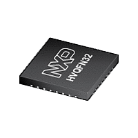
LPC1343FHN33 NXP Semiconductors, LPC1343FHN33 Datasheet - Page 22

LPC1343FHN33
Manufacturer Part Number
LPC1343FHN33
Description
The LPC1343FHN33 is a ARM Cortex-M3 based microcontroller for embedded applications featuring a high level of integration and low power consumption
Manufacturer
NXP Semiconductors
Datasheet
1.LPC1311FHN33.pdf
(73 pages)
Available stocks
Company
Part Number
Manufacturer
Quantity
Price
Company:
Part Number:
LPC1343FHN33
Manufacturer:
SG
Quantity:
200
Part Number:
LPC1343FHN33
Manufacturer:
NXP/恩智浦
Quantity:
20 000
Company:
Part Number:
LPC1343FHN33,551
Manufacturer:
NXP
Quantity:
780
NXP Semiconductors
LPC1311_13_42_43
Product data sheet
7.12.1 Features
7.13.1 Features
7.13 10-bit ADC
The I
(SCL) and a Serial DAta line (SDA). Each device is recognized by a unique address and
can operate as either a receiver-only device (e.g., an LCD driver) or a transmitter with the
capability to both receive and send information (such as memory). Transmitters and/or
receivers can operate in either master or slave mode, depending on whether the chip has
to initiate a data transfer or is only addressed. The I
controlled by more than one bus master connected to it.
The LPC1311/13/42/43 contains one ADC. It is a single 10-bit successive approximation
ADC with eight channels.
•
•
•
•
•
•
•
•
•
•
•
•
•
•
•
•
•
•
The I
pins. The I
Easy to configure as master, slave, or master/slave.
Programmable clocks allow versatile rate control.
Bidirectional data transfer between masters and slaves.
Multi-master bus (no central master).
Arbitration between simultaneously transmitting masters without corruption of serial
data on the bus.
Serial clock synchronization allows devices with different bit rates to communicate via
one serial bus.
Serial clock synchronization can be used as a handshake mechanism to suspend and
resume serial transfer.
The I
The I
10-bit successive approximation ADC.
Input multiplexing among 8 pins.
Power-down mode.
Measurement range 0 V to V
10-bit conversion time 2.44 s (up to 400 kSamples/s).
Burst conversion mode for single or multiple inputs.
Optional conversion on transition of input pin or timer match signal.
Individual result registers for each ADC channel to reduce interrupt overhead.
2
C-bus is bidirectional for inter-IC control using only two wires: a Serial Clock Line
2
2
2
C-bus interface is a standard I
C-bus can be used for test and diagnostic purposes.
C-bus controller supports multiple address recognition and a bus monitor mode.
2
C-bus interface also supports Fast-mode Plus with bit rates up to 1 Mbit/s.
All information provided in this document is subject to legal disclaimers.
Rev. 4 — 20 June 2011
DD
.
2
C-bus compliant interface with true open-drain
32-bit ARM Cortex-M3 microcontroller
2
LPC1311/13/42/43
C is a multi-master bus and can be
© NXP B.V. 2011. All rights reserved.
22 of 73


