BF1102 NXP Semiconductors, BF1102 Datasheet - Page 2
BF1102
Manufacturer Part Number
BF1102
Description
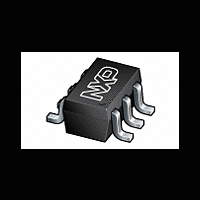
Enhancement type Field-Effect Transistor in a plastic SOT363 package
Manufacturer
NXP Semiconductors
Datasheet
1.BF1102.pdf
(14 pages)
Available stocks
Company
Part Number
Manufacturer
Quantity
Price
Company:

Part Number:
BF1102
Manufacturer:
NXP
Quantity:
24 000
Company:
Part Number:
BF1102
Manufacturer:
PANASONIC
Quantity:
2 186
Company:
Part Number:
BF1102R
Manufacturer:
NXP
Quantity:
24 000
Part Number:
BF1102R
Manufacturer:
NXP/恩智浦
Quantity:
20 000


NXP Semiconductors
FEATURES
Two low noise gain controlled amplifiers in a single
Specially designed for 5 V applications
Superior cross-modulation performance during AGC
High forward transfer admittance
High forward transfer admittance to input capacitance
APPLICATIONS
Gain controlled low noise amplifier for VHF and UHF
applications such as television tuners and professional
communications equipment.
DESCRIPTION
The BF1102 and BF1102R are both two equal dual gate
MOS-FETs which have a shared source pin and a shared
gate 2 pin. Both devices have interconnected source and
substrate; an internal bias circuit enables DC stabilization
and a very good cross-modulation performance at 5 V
supply voltage; integrated diodes between the gates and
source protect against excessive input voltage surges.
Both devices have a SOT363 micro-miniature plastic
package.
QUICK REFERENCE DATA
Note
1. T
2000 Apr 11
Per MOS-FET unless otherwise specified
V
I
P
y
C
C
F
X
T
This product is supplied in anti-static packing to prevent damage caused by electrostatic discharge during transport
and handling.
SYMBOL
D
package
ratio.
j
DS
tot
mod
Dual N-channel dual gate MOS-FETs
ig1-s
rss
fs
s
is the temperature at the soldering point of the source lead.
drain-source voltage
drain current (DC)
total power dissipation
forward transfer admittance
input capacitance at gate 1
reverse transfer capacitance
noise figure
cross-modulation
operating junction temperature
PARAMETER
T
I
I
f = 1 MHz
f = 800 MHz
input level for k = 1% at 40 dB AGC
D
D
s
= 15 mA
= 15 mA
102 C; note 1
CAUTION
CONDITIONS
2
PINNING - SOT363
handbook, halfpage
BF1102 marking code: W1.
BF1102R marking code: W2-.
PIN
1
2
3
4
5
6
1
6
Fig.1 Simplified outline and symbol.
5
2
gate 1 (1)
gate 2 (1 and 2)
drain (1)
drain (2)
source (1 and 2) gate 2 (1 and 2)
gate 1 (2)
4
3
BF1102
g 1 (1)
g 1 (2)
36
100
MIN.
BF1102; BF1102R
DESCRIPTION
g 2 (1, 2)
gate 1 (1)
source (1 and 2)
drain (1)
drain (2)
gate 1 (2)
43
2.8
30
2
AMP2
s (1, 2)
TYP.
Product specification
AMP1
BF1102R
7
40
200
3.6
50
2.8
150
MAX.
MBL029
V
mA
mW
mS
pF
fF
dB
dBV
C
d (1)
d (2)
UNIT
Related parts for BF1102
Image
Part Number
Description
Manufacturer
Datasheet
Request
R

Part Number:
Description:
NXP Semiconductors designed the LPC2420/2460 microcontroller around a 16-bit/32-bitARM7TDMI-S CPU core with real-time debug interfaces that include both JTAG andembedded trace
Manufacturer:
NXP Semiconductors
Datasheet:

Part Number:
Description:
NXP Semiconductors designed the LPC2458 microcontroller around a 16-bit/32-bitARM7TDMI-S CPU core with real-time debug interfaces that include both JTAG andembedded trace
Manufacturer:
NXP Semiconductors
Datasheet:
Part Number:
Description:
NXP Semiconductors designed the LPC2468 microcontroller around a 16-bit/32-bitARM7TDMI-S CPU core with real-time debug interfaces that include both JTAG andembedded trace
Manufacturer:
NXP Semiconductors
Datasheet:
Part Number:
Description:
NXP Semiconductors designed the LPC2470 microcontroller, powered by theARM7TDMI-S core, to be a highly integrated microcontroller for a wide range ofapplications that require advanced communications and high quality graphic displays
Manufacturer:
NXP Semiconductors
Datasheet:
Part Number:
Description:
NXP Semiconductors designed the LPC2478 microcontroller, powered by theARM7TDMI-S core, to be a highly integrated microcontroller for a wide range ofapplications that require advanced communications and high quality graphic displays
Manufacturer:
NXP Semiconductors
Datasheet:
Part Number:
Description:
The Philips Semiconductors XA (eXtended Architecture) family of 16-bit single-chip microcontrollers is powerful enough to easily handle the requirements of high performance embedded applications, yet inexpensive enough to compete in the market for hi
Manufacturer:
NXP Semiconductors
Datasheet:
Part Number:
Description:
The XA-S3 device is a member of Philips Semiconductors? XA(eXtended Architecture) family of high performance 16-bitsingle-chip microcontrollers
Manufacturer:
NXP Semiconductors
Datasheet:

Part Number:
Description:
The NXP BlueStreak LH75401/LH75411 family consists of two low-cost 16/32-bit System-on-Chip (SoC) devices
Manufacturer:
NXP Semiconductors
Datasheet:
Part Number:
Description:
The NXP LPC3130/3131 combine an 180 MHz ARM926EJ-S CPU core, high-speed USB2
Manufacturer:
NXP Semiconductors
Datasheet:
Part Number:
Description:
The NXP LPC3141 combine a 270 MHz ARM926EJ-S CPU core, High-speed USB 2
Manufacturer:
NXP Semiconductors
Part Number:
Description:
The NXP LPC3143 combine a 270 MHz ARM926EJ-S CPU core, High-speed USB 2
Manufacturer:
NXP Semiconductors

Part Number:
Description:
The NXP LPC3152 combines an 180 MHz ARM926EJ-S CPU core, High-speed USB 2
Manufacturer:
NXP Semiconductors
Part Number:
Description:
The NXP LPC3154 combines an 180 MHz ARM926EJ-S CPU core, High-speed USB 2
Manufacturer:
NXP Semiconductors

Part Number:
Description:
Standard level N-channel enhancement mode Field-Effect Transistor (FET) in a plastic package using NXP High-Performance Automotive (HPA) TrenchMOS technology
Manufacturer:
NXP Semiconductors
Datasheet: