CD4503BCN Fairchild Semiconductor, CD4503BCN Datasheet
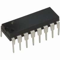
IC BUFF TRI-ST HEX N-INV 16DIP

CD4503BCN

Manufacturer Part Number
CD4503BCN
Description
IC BUFF TRI-ST HEX N-INV 16DIP
Manufacturer
Fairchild Semiconductor
Series
4000Br
Datasheet

Specifications of CD4503BCN

Logic Type
Buffer/Line Driver, Non-Inverting
Number Of Elements
2
Number Of Bits Per Element
2, 4 (Hex)
Current - Output High, Low
17.6mA, 25mA
Voltage - Supply
3 V ~ 18 V
Operating Temperature
-55°C ~ 125°C
Mounting Type
Through Hole
Package / Case
16-DIP (0.300", 7.62mm)
Lead Free Status / RoHS Status
Lead free / RoHS Compliant
Other names
4503
4503B

Available stocks

Company
Part Number
Manufacturer
Quantity
Price
Part Number:
CD4503BCN
Manufacturer:
DENSO
Quantity:
6 247
Part Number:
CD4503BCN
Manufacturer:
NS/国半
Quantity:
20 000
© 2004 Fairchild Semiconductor Corporation
CD4503BCM
CD4503BCN
CD4503BC
Hex Non-Inverting 3-STATE Buffer
General Description
The CD4503BC is a hex non-inverting 3-STATE buffer with
high output current sink and source capability. 3-STATE
outputs make it useful in bus-oriented applications. Two
separate disable inputs are provided. Buffers 1 through 4
are controlled by the disable 4 input. Buffers 5 and 6 are
controlled by the disable 2 input. A high level on either dis-
able input will cause those gates on its control line to go
into a high impedance state.
Ordering Code:
Connection Diagram
Order Number
Package Number
Top View
M16A
N16E
16-Lead Small Outline Integrated Circuit (SOIC), JEDEC MS-012, 0.150" Narrow
16-Lead Plastic Dual-In-Line Package (PDIP), JEDEC MS-001, 0.300" Wide
DS005989
Features
Schematic Diagram
Truth Table
X
Wide supply voltage range:
3-STATE outputs
Symmetrical turn on/turn off delays
Symmetrical output rise and fall times
Pin-for-pin replacement for MM80C97 and MC14503
Don’t Care
Package Description
In
X
0
1
Disable
Input
0
1
0
October 1987
Revised January 2004
3.0 V
DC
www.fairchildsemi.com
3-STATE
to 18 V
Out
0
1
DC

Related parts for CD4503BCN

CD4503BCN Summary of contents

Page 1

... Ordering Code: Order Number Package Number CD4503BCM M16A 16-Lead Small Outline Integrated Circuit (SOIC), JEDEC MS-012, 0.150" Narrow CD4503BCN N16E 16-Lead Plastic Dual-In-Line Package (PDIP), JEDEC MS-001, 0.300" Wide Connection Diagram Top View © 2004 Fairchild Semiconductor Corporation Features ...

Page 2

Absolute Maximum Ratings (Note 2) Supply Voltage ( Input Voltage ( Storage Temperature Range ( Power Dissipation ( Dual-In-Line Small Outline Lead Temperature ( (Soldering, 10 seconds) DC Electrical Characteristics ...

Page 3

AC Electrical Characteristics pF, R 200 k , Input Symbol Parameter Propagation Delay Time PHL PLH Propagation Delay Time, PLZ PHZ Logical Level to HIGH ...

Page 4

AC Test Circuits and Switching Time Waveforms PHL PLH t and t PHZ PZH t PHZ t PZH Note: Delays measured with input ns www.fairchildsemi.com CMOS to CMOS t and t ...

Page 5

Physical Dimensions inches (millimeters) unless otherwise noted 16-Lead Small Outline Integrated Circuit (SOIC), JEDEC MS-012, 0.150" Narrow Package Number M16A 5 www.fairchildsemi.com ...

Page 6

Physical Dimensions inches (millimeters) unless otherwise noted (Continued) 16-Lead Plastic Dual-In-Line Package (PDIP), JEDEC MS-001, 0.300" Wide Fairchild does not assume any responsibility for use of any circuitry described, no circuit patent licenses are implied and Fairchild reserves the right ...

Related keywords