CD4503BCN Fairchild Semiconductor, CD4503BCN Datasheet - Page 2
CD4503BCN
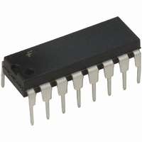
Manufacturer Part Number
CD4503BCN
Description
IC BUFF TRI-ST HEX N-INV 16DIP
Manufacturer
Fairchild Semiconductor
Series
4000Br
Datasheet
1.CD4503BCN.pdf
(6 pages)
Specifications of CD4503BCN
Logic Type
Buffer/Line Driver, Non-Inverting
Number Of Elements
2
Number Of Bits Per Element
2, 4 (Hex)
Current - Output High, Low
17.6mA, 25mA
Voltage - Supply
3 V ~ 18 V
Operating Temperature
-55°C ~ 125°C
Mounting Type
Through Hole
Package / Case
16-DIP (0.300", 7.62mm)
Lead Free Status / RoHS Status
Lead free / RoHS Compliant
Other names
4503
4503B
4503B
Available stocks
Company
Part Number
Manufacturer
Quantity
Price
Company:

Part Number:
CD4503BCN
Manufacturer:
DENSO
Quantity:
6 247
Part Number:
CD4503BCN
Manufacturer:
NS/国半
Quantity:
20 000


www.fairchildsemi.com
I
V
V
V
I
I
I
I
DD
V
OL
OH
OZ
IN
Symbol
Absolute Maximum Ratings
(Note 2)
DC Electrical Characteristics
Note 3: I
OL
IL
IH
Supply Voltage (V
Input Voltage (V
Storage Temperature Range (T
Power Dissipation (P
Lead Temperature (T
OH
Dual-In-Line
Small Outline
(Soldering, 10 seconds)
OH
Quiescent Device
Current
LOW Level
Output Voltage
HIGH Level
Output Voltage
LOW Level
Input Voltage
HIGH Level
Input Voltage
LOW Level Output
Current
HIGH Level Output
Current
3-STATE Leakage Current
Input Current
and I
OL
are tested one output at a time.
IN
Parameter
)
DD
)
D
L
)
)
S
)
V
V
V
V
V
V
V
V
V
V
V
V
V
V
V
V
V
V
V
V
V
V
V
V
V
V
V
V
V
V
V
V
V
V
V
DD
IN
DD
IN
DD
IN
IN
DD
DD
DD
IN
DD
DD
DD
DD
O
DD
O
DD
O
DD
O
DD
O
DD
O
DD
DD
DD
DD
DD
DD
DD
DD
DD
4.5V or 0.5V
9.0V or 1.0V
13.5V or 1.5V
0.5V or 4.5V
1.0V or 9.0V
1.5V or 13.5V
V
V
V
V
V
5V,
10V,
15V,
5V
10V
15V
5V
10V
15V
5V,
10V,
15V,
5V,
10V,
15V,
4.5V, V
5.0V, V
10V, V
15V, V
5V, V
10V, V
15V, V
15V
15V
65 C to 150 C
DD
DD
DD
DD
DD
0.5V to 0.5V
(Note 1)
0.5V to 18V
or V
or V
or V
or 0
or 0
Conditions
OH
OL
OH
OH
(Note 2)
OL
OL
OL
SS
SS
SS
700 mW
500 mW
4.6V
260 C
1.5V
9.5V
13.5V
0.5V
0.4V
0.4V
2
Recommended Operating
Conditions
Note 1: “Absolute Maximum Ratings” are those values beyond which the
safety of the device cannot be guaranteed. They are not meant to imply
that the devices should be operated at these limits. The tables of “Recom-
mended Operating Conditions” and “Electrical Characteristics” provide con-
ditions for actual device operation.
Note 2: V
Supply Voltage (V
Operating Temperature Range (T
14.95
19.95
4.95
9.95
7.85
Min
11.0
3.5
7.0
2.8
3.0
1.28
3.20
8.20
SS
55 C
0V unless otherwise specified.
Max
0.05
0.05
0.05
1.5
3.0
4.0
0.1
0.1
1
2
4
DD
14.95
16.10
(Note 2)
4.95
9.95
11.0
6.35
Min
7.0
2.3
1.02
2.60
6.80
3.5
2.4
)
25.00
4.50
6.75
2.75
8.25
2.55
2.75
7.00
Typ
2.25
25 C
5.5
1.76
17.6
10
10
10
15
4.5
0
0
0
5
4
4
A
Max
0.05
0.05
0.05
1.5
3.0
4.0
)
0.1
0.1
2
4
1
11.30
14.95
1.60
1.75
Min
4.95
9.95
11.0
4.45
3.5
7.0
0.7
1.8
4.8
55 C to 125 C
125 C
3V to 15V
Max
0.05
0.05
0.05
120
1.5
3.0
4.0
30
60
1.0
1.0
Units
mA
mA
V
V
V
V
A
A
A
Related parts for CD4503BCN
Image
Part Number
Description
Manufacturer
Datasheet
Request
R

Part Number:
Description:
Fairchild Semiconductor [IGBT MODULE]
Manufacturer:
Fairchild Semiconductor
Datasheet:

Part Number:
Description:
Discrete Semiconductor Modules
Manufacturer:
Fairchild Semiconductor
Part Number:
Description:
Discrete Semiconductor Modules
Manufacturer:
Fairchild Semiconductor
Part Number:
Description:
This N-Channel MOSFET is produced using Fairchild Semiconductor’s advanced Power Trench® process
Manufacturer:
Fairchild Semiconductor
Datasheet:
Part Number:
Description:
This N-Channel MOSFET is produced using Fairchild Semiconductor’s advanced Power Trench® process
Manufacturer:
Fairchild Semiconductor
Datasheet:
Part Number:
Description:
This N-Channel MOSFET is produced using Fairchild Semiconductor’s advanced PowerTrench® process
Manufacturer:
Fairchild Semiconductor
Datasheet:
Part Number:
Description:
This N-Channel MOSFET is produced using Fairchild Semiconductor’s advanced PowerTrench® process
Manufacturer:
Fairchild Semiconductor
Datasheet:
Part Number:
Description:
This N-Channel MOSFET is produced using Fairchild Semiconductor’s advanced Power Trench® process
Manufacturer:
Fairchild Semiconductor
Datasheet:
Part Number:
Description:
This N-Channel logic Level MOSFETs are produced using Fairchild Semiconductor‘s advanced Power Trench® process that has been special tailored to minimize the on-state resistance and yet maintain superior switching performance
Manufacturer:
Fairchild Semiconductor
Datasheet:
Part Number:
Description:
This N-Channel MOSFET is produced using Fairchild Semiconductor’s advanced Power Trench® process
Manufacturer:
Fairchild Semiconductor
Datasheet:
Part Number:
Description:
This N-Channel SyncFET™ is produced using Fairchild Semiconductor’s advanced PowerTrench® process
Manufacturer:
Fairchild Semiconductor
Datasheet:
Part Number:
Description:
This N-Channel SyncFET™ is produced using Fairchild Semiconductor’s advanced PowerTrench® process
Manufacturer:
Fairchild Semiconductor
Datasheet:
Part Number:
Description:
This N-Channel SyncFET™ is produced using Fairchild Semiconductor’s advanced PowerTrench® process
Manufacturer:
Fairchild Semiconductor
Datasheet:
Part Number:
Description:
This N-Channel logic Level MOSFETs are produced using Fairchild Semiconductor‘s advanced Power Trench® process that has been special tailored to minimize the on-state resistance and yet maintain superior switching performance
Manufacturer:
Fairchild Semiconductor
Datasheet:
Part Number:
Description:
This N-Channel MOSFET is produced using Fairchild Semiconductor’s advanced Power Trench® process that has been especially tailored to minimize the on-state resistance and yet maintain superior switching performance
Manufacturer:
Fairchild Semiconductor
Datasheet: