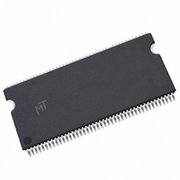
MT48LC4M32B2TG-7:G Micron Technology Inc, MT48LC4M32B2TG-7:G Datasheet - Page 17

MT48LC4M32B2TG-7:G
Manufacturer Part Number
MT48LC4M32B2TG-7:G
Description
IC SDRAM 128MBIT 143MHZ 86TSOP
Manufacturer
Micron Technology Inc
Type
SDRAMr
Datasheet
1.MT48LC4M32B2P-7G_TR.pdf
(67 pages)
Specifications of MT48LC4M32B2TG-7:G
Format - Memory
RAM
Memory Type
SDRAM
Memory Size
128M (4Mx32)
Speed
143MHz
Interface
Parallel
Voltage - Supply
3 V ~ 3.6 V
Operating Temperature
0°C ~ 70°C
Package / Case
86-TSOPII
Organization
4Mx32
Density
128Mb
Address Bus
14b
Access Time (max)
17/8/5.5ns
Maximum Clock Rate
143MHz
Operating Supply Voltage (typ)
3.3V
Package Type
TSOP-II
Operating Temp Range
0C to 70C
Operating Supply Voltage (max)
3.6V
Operating Supply Voltage (min)
3V
Supply Current
175mA
Pin Count
86
Mounting
Surface Mount
Operating Temperature Classification
Commercial
Lead Free Status / RoHS Status
Contains lead / RoHS non-compliant
Available stocks
Company
Part Number
Manufacturer
Quantity
Price
Company:
Part Number:
MT48LC4M32B2TG-7:G
Manufacturer:
micron
Quantity:
415
Part Number:
MT48LC4M32B2TG-7:G
Manufacturer:
MICRONAS
Quantity:
20 000
Commands
Table 8:
COMMAND INHIBIT
NO OPERATION (NOP)
PDF: 09005aef80872800/Source: 09005aef80863355
128MbSDRAMx32_2.fm - Rev. L 1/09 EN
NAME (FUNCTION)
COMMAND INHIBIT (NOP)
NO OPERATION (NOP)
ACTIVE (Select bank and activate row)
READ (Select bank and column, and start READ burst)
WRITE (Select bank and column, and start WRITE burst)
BURST TERMINATE
PRECHARGE (Deactivate row in bank or banks)
AUTO REFRESH or SELF REFRESH
(Enter self refresh mode)
LOAD MODE REGISTER
Write Enable/Output Enable
Write Inhibit/Output High-Z
Truth Table–Commands and DQM Operation
Note 1 applies to the entire table
Notes:
Table 8 provides a quick reference of available commands. This is followed by a written
description of each command. Three additional Truth Tables appear following the Oper-
ation section; these tables provide current state/next state information.
1. CKE is HIGH for all commands shown except SELF REFRESH.
2. A0–A11 define the op-code written to the mode register.
3. A0–A11 provide row address, BA0 and BA1 determine which bank is made active.
4. A0–A7 provide column address; A10 HIGH enables the auto precharge feature (nonpersis-
5. A10 LOW: BA0 and BA1 determine the bank being precharged. A10 HIGH: All banks pre-
6. This command is AUTO REFRESH if CKE is HIGH; SELF REFRESH if CKE is LOW.
7. Internal refresh counter controls row addressing; all inputs and I/Os are “Don’t Care” except
8. Activates or deactivates the DQs during WRITEs (zero-clock delay) and READs (two-clock
The COMMAND INHIBIT function prevents new commands from being executed by the
SDRAM, regardless of whether the CLK signal is enabled. The SDRAM is effectively dese-
lected. Operations already in progress are not affected.
The NO OPERATION (NOP) command is used to perform a NOP to an SDRAM which is
selected (CS# is LOW). This prevents unwanted commands from being registered during
idle or wait states. Operations already in progress are not affected.
tent), while A10 LOW disables the auto precharge feature; BA0 and BA1 determine which
bank is being read from or written to.
charged and BA0 and BA1 are “Don’t Care.”
for CKE.
delay). DQM0 controls DQ0–DQ7; DQM1 controls DQ8–DQ15; DQM2 controls DQ16–DQ23;
and DQM3 controls DQ24–DQ31.
CS# RAS# CAS# WE# DQM
H
L
L
L
L
L
L
L
–
–
L
17
H
H
H
H
X
L
L
L
L
–
–
Micron Technology, Inc., reserves the right to change products or specifications without notice.
H
H
H
H
X
L
L
L
L
–
–
H
H
H
H
X
L
L
L
L
–
–
L/H8
L/H8
H
X
X
X
X
X
X
X
L
Bank/Row
Bank/Col
Bank/Col
Op-Code
©2001 Micron Technology, Inc. All rights reserved.
128Mb: x32 SDRAM
ADDR
Register Definition
Code
X
X
X
X
–
–
High-Z
Active
Active
Valid
DQs
X
X
X
X
X
X
X
NOTES
6, 7
3
4
4
5
2
8
8


