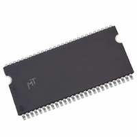
MT46V64M16TG-6T IT:A TR Micron Technology Inc, MT46V64M16TG-6T IT:A TR Datasheet - Page 13

MT46V64M16TG-6T IT:A TR
Manufacturer Part Number
MT46V64M16TG-6T IT:A TR
Description
IC DDR SDRAM 1GBIT 6NS 66TSOP
Manufacturer
Micron Technology Inc
Type
DDR SDRAMr
Datasheet
1.MT46V256M4P-6TA_TR.pdf
(82 pages)
Specifications of MT46V64M16TG-6T IT:A TR
Format - Memory
RAM
Memory Type
DDR SDRAM
Memory Size
1G (64M x 16)
Speed
6ns
Interface
Parallel
Voltage - Supply
2.3 V ~ 2.7 V
Operating Temperature
-40°C ~ 85°C
Package / Case
66-TSOP
Organization
64Mx16
Density
1Gb
Address Bus
16b
Access Time (max)
700ps
Maximum Clock Rate
333MHz
Operating Supply Voltage (typ)
2.5V
Package Type
TSOP
Operating Temp Range
-40C to 85C
Operating Supply Voltage (max)
2.7V
Operating Supply Voltage (min)
2.3V
Supply Current
275mA
Pin Count
66
Mounting
Surface Mount
Operating Temperature Classification
Industrial
Lead Free Status / RoHS Status
Lead free / RoHS Compliant
Table 6:
PDF: 09005aef80a2f898/Source: 09005aef82a95a3a
1Gb_DDR_x4x8x16_D2.fm - 1Gb DDR: Rev. I, Core DDR: Rev. B 12/07 EN
Parameter/Condition
Operating one-bank active-precharge current:
t
changing once per clock cycle; Address and control inputs
changing once every two clock cycles
Operating one-bank active-read-precharge current:
BL = 4;
Address and control inputs changing once per clock cycle
Precharge power-down standby current: All banks
idle; Power-down mode;
Idle standby current: CS# = HIGH; All banks are idle;
t
inputs changing once per clock cycle. V
DQS, and DM
Active power-down standby current: One bank
active; Power-down mode;
Active standby current: CS# = HIGH; CKE = HIGH; One
bank active;
and DQS inputs changing twice per clock cycle; Address
and other control inputs changing once per clock cycle
Operating burst read current: BL = 2;
reads; One bank active; Address and control inputs changing
once per clock cycle;
Operating burst write current: BL = 2; Continuous
burst writes; One bank active; Address and control inputs
changing once per clock cycle;
and DQS inputs changing twice per clock cycle
Auto refresh burst current:
Self refresh current: CKE ≤ 0.2V
Operating bank interleave read current: Four bank
interleaving READs (BL = 4) with auto precharge;
t
change only during ACTIVE, READ, or WRITE commands
RC =
CK =
RC = MIN;
t
t
RC (MIN);
CK (MIN); CKE = HIGH; Address and other control
t
RC =
t
CK =
t
I
Notes 1–5, 11, 13, 15, 47 apply to the entire table; Notes appear on page 26–31; See also Table 7 on page 14;
V
0°C ≤ T
t
RC =
DD
RC (MIN);
DD
t
Q = +2.6V ±0.1V, V
Specifications and Conditions (x16)
CK =
t
CK (MIN); Address and control inputs
t
RAS (MAX);
A
t
CK =
≤ +70°C
t
CK (MIN); DQ, DM and DQS inputs
t
CK =
t
t
CK =
CK (MIN);
t
CK =
t
CK (MIN); I
t
t
t
CK =
CK (MIN); CKE = LOW
CK =
t
CK (MIN); CKE = LOW
DD
I
OUT
t
= +2.6V ±0.1V (-5B); V
t
CK (MIN); DQ, DM,
CK (MIN); DQ, DM,
IN
t
t
Standard
= 0mA
REFC =
REFC = 7.8µs
Continuous burst
OUT
= V
REF
= 0mA;
t
for DQ,
RFC (MIN)
13
DD
Q = +2.5V ±0.2V, V
Symbol
I
I
I
I
I
I
I
DD
DD
DD
I
I
DD
DD
DD
I
I
I
DD
DD
DD
DD
DD
DD
4W
3N
5A
4R
2P
2F
3P
0
1
5
6
7
Micron Technology, Inc., reserves the right to change products or specifications without notice.
-5B
170
215
280
285
345
545
15
70
40
55
15
10
Electrical Specifications – I
DD
1Gb: x4, x8, x16 DDR SDRAM
= +2.5V ±0.2V (-6T, -75);
165
210
270
275
340
535
-6T
10
65
35
50
10
9
©2003 Micron Technology, Inc. All rights reserved.
-75
145
195
245
250
330
495
10
60
30
45
10
9
Units
mA
mA
mA
mA
mA
mA
mA
mA
mA
mA
mA
mA
Notes
23, 48
23, 48
24, 33
24, 33
23, 48
28, 50
23, 49
51
23
23
50
12
DD


