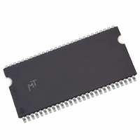
MT46V64M16TG-6T IT:A TR Micron Technology Inc, MT46V64M16TG-6T IT:A TR Datasheet - Page 7

MT46V64M16TG-6T IT:A TR
Manufacturer Part Number
MT46V64M16TG-6T IT:A TR
Description
IC DDR SDRAM 1GBIT 6NS 66TSOP
Manufacturer
Micron Technology Inc
Type
DDR SDRAMr
Datasheet
1.MT46V256M4P-6TA_TR.pdf
(82 pages)
Specifications of MT46V64M16TG-6T IT:A TR
Format - Memory
RAM
Memory Type
DDR SDRAM
Memory Size
1G (64M x 16)
Speed
6ns
Interface
Parallel
Voltage - Supply
2.3 V ~ 2.7 V
Operating Temperature
-40°C ~ 85°C
Package / Case
66-TSOP
Organization
64Mx16
Density
1Gb
Address Bus
16b
Access Time (max)
700ps
Maximum Clock Rate
333MHz
Operating Supply Voltage (typ)
2.5V
Package Type
TSOP
Operating Temp Range
-40C to 85C
Operating Supply Voltage (max)
2.7V
Operating Supply Voltage (min)
2.3V
Supply Current
275mA
Pin Count
66
Mounting
Surface Mount
Operating Temperature Classification
Industrial
Lead Free Status / RoHS Status
Lead free / RoHS Compliant
Figure 4:
Figure 5:
PDF: 09005aef80a2f898/Source: 09005aef82a95a3a
1Gb_DDR_x4x8x16_D2.fm - 1Gb DDR: Rev. I, Core DDR: Rev. B 12/07 EN
128 Meg x 8 Functional Block Diagram
64 Meg x 16 Functional Block Diagram
BA0, BA1
BA0, BA1
A0–A13,
A0–A13,
RAS#
CAS#
WE#
CAS#
RAS#
CKE
CK#
WE#
CS#
CKE
CK#
CK
CS#
CK
16
16
Address
register
Address
register
Mode registers
Mode registers
Control
Control
logic
16
logic
16
counter
14
Refresh
14
counter
Refresh
10
11
2
2
13
13
address
2
address
2
Row-
MUX
Row-
MUX
Column-
counter/
control
address
Column-
counter/
14
Bank
address
logic
latch
control
14
Bank
logic
latch
decoder
address
Bank 0
decoder
address
row-
latch
Bank 0
row-
latch
&
&
9
1
10
1
16,384
16,384
7
SENSE AMPLIFIERS
(16,384 x 512 x 32)
(16,384 x 1,024 x 16)
SENSE AMPLIFIERS
DM mask logic
DM mask logic
I/O gating
Column
decoder
I/O gating
memory
Bank 0
decoder
memory
Column
array
512
Bank 0
Bank 1
1024
array
Bank 1
Micron Technology, Inc., reserves the right to change products or specifications without notice.
Bank 2
Bank 2
(16,384)
(16,384)
Bank 3
Bank 3
32
16
32
16
1Gb: x4, x8, x16 DDR SDRAM
32
16
READ
latch
READ
latch
Functional Block Diagrams
out
CK
CK
CLK
out
CK
drivers
WRITE
FIFO
and
WRITE
drivers
16
16
FIFO
and
8
8
CK
in
CLK
in
Column 0
Column 0
MUX
Mask
Data
Column 0
MUX
Mask
Data
Column 0
32
4
16
2
©2003 Micron Technology, Inc. All rights reserved.
2
2
16
16
1
1
8
8
generator
registers
generator
Input
registers
DQS
Input
16
DQS
8
2
2
16
16
Data
1
1
8
8
Data
2
2
32
1
1
8
1
DQS
DRVRS
1
DQS
DLL
CK
DRVRS
RCVRS
DLL
CK
RCVRS
DQ0–DQ15
DQS L/H
LDM, UDM
DQ0–DQ7
DQS
DM


