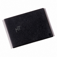
MT28F320J3RG-11 GMET Micron Technology Inc, MT28F320J3RG-11 GMET Datasheet - Page 10

MT28F320J3RG-11 GMET
Manufacturer Part Number
MT28F320J3RG-11 GMET
Description
IC FLASH 32MBIT 110NS 56TSOP
Manufacturer
Micron Technology Inc
Datasheet
1.MT28F128J3FS-12_ET_TR.pdf
(55 pages)
Specifications of MT28F320J3RG-11 GMET
Format - Memory
FLASH
Memory Type
FLASH
Memory Size
32M (4Mx8, 2Mx16)
Speed
110ns
Interface
Parallel
Voltage - Supply
2.7 V ~ 3.6 V
Operating Temperature
-40°C ~ 85°C
Package / Case
56-TSOP
Lead Free Status / RoHS Status
Contains lead / RoHS non-compliant
Table 1:
09005aef80b5a323
MT28F640J3.fm – Rev. N 3/05 EN
13, 12, 11, 10, 8,
32, 28, 27, 26,
25, 24, 23, 22,
20, 19, 18, 17,
7, 6, 5, 4, 3, 1,
33, 35, 38, 40,
44, 46, 49, 51,
34, 36, 39, 41,
56-PIN TSOP
45, 47, 50, 52
NUMBERS
21, 42, 48
14, 2, 29
1, 30, 56
9, 37
55
16
54
30
31
15
53
43
—
Pin/Ball Descriptions
64-BALL FBGA
D1, D2, A2, C2,
D7, D8, A7, B7,
G2, A1, B1, C1,
A3, B3, C3, D3,
E5, G5, G6, H7,
B6, C6, D5, D6,
C4, A5, B5, C5,
C7, C8, A8, G1
F2, E2, G3, E4,
E1, E3, F3, F4,
F5, H5, G7, E7
E6, F6, F7, H2
NUMBERS
A1, G1, H8
B2, H4, H6
B4, B8, H1
H3, A6
G8
D4
A4
G4
F8
F1
E8
SYMBOL
CE0, CE1,
A0−A21/
BYTE#
DQ15
(A22)
(A23)
DQ0–
V
WE#
V
DNU
OE#
CE2
RP#
V
STS
V
NC
CC
PEN
CC
SS
Q
Output
Output Status: Indicates the status of the ISM. When configured in level
Supply V
Supply Power Supply: 2.7V to 3.6V.
Supply Ground.
Input/
TYPE
Input
Input
Input
Input
Input
Input
Input
—
—
Write Enable: Determines if a given cycle is a WRITE cycle. If WE# is
LOW, the cycle is either a WRITE to the command execution logic
(CEL) or to the memory array. Addresses and data are latched on
the rising edge of the WE# pulse.
Chip Enable: Three CE pins enable the use of multiple Flash devices
in the system without requiring additional logic. The device can be
configured to use a single CE signal by tying CE1 and CE2 to
ground and then using CE0 as CE. Device selection occurs with the
first edge of CE0, CE1, or CE2 (CEx) that enables the device. Device
deselection occurs with the first edge of CEx that disables the
device (see Table 2 on page 11).
Reset/Power-Down: When LOW, RP# clears the status register, sets
the ISM to the array read mode, and places the device in deep
power-down mode. All inputs, including CEx, are “Don’t Care,”
and all outputs are High-Z. RP# must be held at V
other modes of operation.
Output Enables: Enables data ouput buffers when LOW. When
OE# is HIGH, the output buffers are disabled.
Address inputs during READ and WRITE operations.
A0 is only used in x8 mode and will be a NC in x16 mode (the input
buffer is turned off when BYTE = HIGH).
A22 (pin 1, ball A8) is only available on the 64Mb and 128Mb
devices.
A23 (pin 30, ball G1) is only available on the 128Mb device.
BYTE# low places the device in the x8 mode. BYTE# high places the
device in the x16 mode and turns off the A0 input buffer. Address
A1 becomes the lowest order address in x16 mode.
Necessary voltage for erasing blocks, programming data, or
configuring lock bits. Typically, V
V
Data I/O: Data output pins during any READ operation or data
input pins during a WRITE. DQ8–DQ15 are not used in byte mode
(BYTE = LOW).
mode (default), STS acts as a RY/BY# pin. When configured in its
pulse mode, it can pulse to indicate program and/or erase
completion. Tie STS to V
compatible with system data bus voltages, connect V
system supply voltage.
No Connect: These may be driven or left unconnected. Pin 1 and
ball A8 are NCs on the 32Mb device. Pin 30 and ball G1 are NCs on
the 32Mb and 64Mb devices.
Do Not Use: Must float to minimize noise.
PEN
CC
Q controls the output voltages. To obtain output voltage
10
≤ V
PENLK
, this pin enables hardware write protect.
Micron Technology, Inc., reserves the right to change products or specifications without notice.
CC
DESCRIPTION
Q through a pull-up resistor.
128Mb, 64Mb, 32Mb
Q-FLASH MEMORY
PEN
is connected to V
IH
©2000 Micron Technology. Inc.
during all
CC
CC
Q to the
. When


