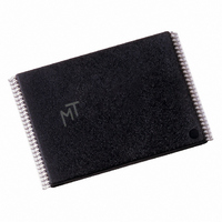
MT28F320J3RG-11 GMET Micron Technology Inc, MT28F320J3RG-11 GMET Datasheet - Page 31

MT28F320J3RG-11 GMET
Manufacturer Part Number
MT28F320J3RG-11 GMET
Description
IC FLASH 32MBIT 110NS 56TSOP
Manufacturer
Micron Technology Inc
Datasheet
1.MT28F128J3FS-12_ET_TR.pdf
(55 pages)
Specifications of MT28F320J3RG-11 GMET
Format - Memory
FLASH
Memory Type
FLASH
Memory Size
32M (4Mx8, 2Mx16)
Speed
110ns
Interface
Parallel
Voltage - Supply
2.7 V ~ 3.6 V
Operating Temperature
-40°C ~ 85°C
Package / Case
56-TSOP
Lead Free Status / RoHS Status
Contains lead / RoHS non-compliant
NOTE:
09005aef80b5a323
MT28F640J3.fm – Rev. N 3/05 EN
1. Issuing a READ STATUS REGISTER command (70h) will result in an invalid WRITE BUFFER command.
2. Byte or word count values on DQ0–DQ7 are loaded into the count register. Count ranges on this device for byte
3. The device now outputs the status register when read (XSR is no longer available).
4. Write buffer contents will be programmed at the device start address or destination Flash address.
5. Align the start address on a write buffer boundary for maximum programming performance (i.e., A4–A0 of the
6. The device aborts the WRITE-to-BUFFER command if the current address is outside of the original block address.
7. The status register indicates an “improper command sequence” if the WRITE-to-BUFFER command is aborted. Fol-
8. Toggling OE# (LOW to HIGH to LOW) updates the status register. This must be done in place of issuing the READ
Figure 9: WRITE-to-BUFFER Flowchart
mode are n = 00h to 1Fh and for word mode are n = 0000h to 000Fh.
start address = 0).
low this with a CLEAR STATUS REGISTER command.
STATUS REGISTER command.
Yes
Yes
Data, Device Address
Read Status Register
Program Buffer to
Write Buffer Data,
Write Next Buffer
Flash Confirm D0h
WRITE-to-BUFFER
WRITE-to-BUFFER
WRITE-to-BUFFER
Check if Desired
Yes
Command E8h,
Write Word or
Block Address
Read Extended
Status Register
Byte Count N,
Block Address
Programming
Start Address
Set Timeout
Command?
Full Status
Complete
X = X + 1
Another
XSR7 =
X = N?
Check
Abort
SR7 =
X = 0
Start
Issue
?
No
No
No
1
1
1
Yes
0
0
No
Write to Another
Write to Buffer
Block Address
BUFFER Timeout?
Aborted
WRITE-to-
READ STATUS
Command
Issue
Yes
31
BUS
OPERATION COMMAND COMMENTS
WRITE
READ
STANDBY
WRITE
WRITE
WRITE
WRITE
READ
STANDBY
Full status check can be done after all erase and write sequences
complete. Write FFh after the last operation to reset the device
to read array mode.
Micron Technology, Inc., reserves the right to change products or specifications without notice.
WRITE-to-
BUFFER
Program
Buffer to
Flash
Confirm
128Mb, 64Mb, 32Mb
Q-FLASH MEMORY
Data = E8h
Block Address
XSR7 = Valid
Addr = Block Address
Check XSR7
1 = Write Buffer Available
0 = Write Buffer Not
Available
Data = N = Word/Byte
Count
N = 0 Corresponds to Count
= 1
Addr = Block Address
Data = Write Buffer Data
Addr = Device Start
Address
Data = Write Buffer Data
Addr = Device Address
Data = D0h
Addr = Block Address
Status register data with
the device enabled, OE#
LOW updates the SR
Addr = Block Address
Check SR7
1 = ISM Ready
0 = ISM Busy
©2000 Micron Technology. Inc.
NOTES
1
2, 3
4, 5
6, 7
8


