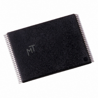
MT28F320J3RG-11 GMET Micron Technology Inc, MT28F320J3RG-11 GMET Datasheet - Page 25

MT28F320J3RG-11 GMET
Manufacturer Part Number
MT28F320J3RG-11 GMET
Description
IC FLASH 32MBIT 110NS 56TSOP
Manufacturer
Micron Technology Inc
Datasheet
1.MT28F128J3FS-12_ET_TR.pdf
(55 pages)
Specifications of MT28F320J3RG-11 GMET
Format - Memory
FLASH
Memory Type
FLASH
Memory Size
32M (4Mx8, 2Mx16)
Speed
110ns
Interface
Parallel
Voltage - Supply
2.7 V ~ 3.6 V
Operating Temperature
-40°C ~ 85°C
Package / Case
56-TSOP
Lead Free Status / RoHS Status
Contains lead / RoHS non-compliant
CLEAR STATUS REGISTER Command
and SR1 to “1s.” These bits, which indicate various fail-
ure conditions, can only be reset by the CLEAR STA-
TUS REGISTER command. Allowing system software
to reset these bits can perform several operations
(such as cumulatively erasing or locking multiple
blocks or writing several bytes in sequence). To deter-
mine if an error occurred during the sequence, the sta-
tus register may be polled. To clear the status register,
the CLEAR STATUS REGISTER command (50h) is writ-
ten. The CLEAR STATUS REGISTER command func-
tions independently of the applied V
only valid when the ISM is off or the device is sus-
pended.
BLOCK ERASE Command
mand that erases one block. First, a block erase setup
is written, followed by a block erase confirm. This
command sequence requires an appropriate address
within the block to be erased. The ISM handles all
block preconditioning, erase, and verify. Time tWB
after the two-cycle block erase sequence is written, the
device automatically outputs status register data when
read. The CPU can detect block erase completion by
analyzing the output of the STS pin or status register
bit SR7. Toggle OE# or CEx to update the status regis-
ter. Upon block erase completion, status register bit
SR5 should be checked to detect any block erase error.
When an error is detected, the status register should be
cleared before system software attempts corrective
actions. The CEL remains in read status register mode
until a new command is issued. This two-step setup
command sequence ensures that block contents are
not accidentally erased. An invalid block erase com-
mand sequence results in status register bits SR4 and
SR5 being set to “1.” Also, reliable block erasure can
only occur when V
that SR3 and SR5 are set to “1” if block erase is
attempted while V
requires that the corresponding block lock bit be
cleared. Similarly, SR1 and SR5 are set to “1” if block
erase is attempted when the corresponding block lock
bit is set.
09005aef80b5a323
MT28F640J3.fm – Rev. N 3/05 EN
The ISM sets the status register bits SR5, SR4, SR3,
The BLOCK ERASE command is a two-cycle com-
PEN
CC
is valid and V
≤ V
PENLK
. Successful block erase
PEN
PEN
= V
voltage and is
PENH
. Note
25
BLOCK ERASE SUSPEND Command
block erase interruption in order to read or program
data in another block of memory. Writing the BLOCK
ERASE SUSPEND command immediately after starting
the block erase process requests that the ISM suspend
the block erase sequence at an appropriate point in
the algorithm. When reading after the BLOCK ERASE
SUSPEND command is written, the device outputs sta-
tus register data. Polling status register bit SR7, fol-
lowed by SR6, shows when the BLOCK ERASE
operation has been suspended. In the default mode,
STS also transitions to V
erase suspend latency. At this point, a READ ARRAY
command can be written to read data from blocks
other than that which is suspended. During erase sus-
pend to program data in other blocks, a program com-
mand sequence can also be issued. During a
PROGRAM operation with block erase suspended, sta-
tus register bit SR7 returns to “0” and STS output (in
default mode) transitions to V
remains “1” to indicate block erase suspend status.
Using the PROGRAM SUSPEND command, a program
operation can also be suspended. Resuming a SUS-
PENDED programming operation by issuing the Pro-
gram Resume command enables the suspended
programming operation to continue. To resume the
suspended erase, the user must wait for the program-
ming operation to complete before issuing the Block
ERASE RESUME command. While block erase is sus-
pended, the only other valid commands are READ
QUERY, READ STATUS REGISTER, CLEAR STATUS
REGISTER,
RESUME. After a BLOCK ERASE RESUME command to
the Flash memory is completed, the ISM continues the
block erase process. Status register bits SR6 and SR7
automatically clear and STS (in default mode) returns
to V
pleted, the device automatically outputs status register
data when read. V
V
pension. Block erase cannot resume during block
erase suspend until PROGRAM operations are com-
plete.
PEN
The BLOCK ERASE SUSPEND command allows
OL
level used for block erase) during block erase sus-
Micron Technology, Inc., reserves the right to change products or specifications without notice.
. After the ERASE RESUME command is com-
CONFIGURE,
PEN
128Mb, 64Mb, 32Mb
must remain at V
Q-FLASH MEMORY
OH
.
t
and
LES defines the block
OL
. However, SR6
BLOCK
©2000 Micron Technology. Inc.
PENH
(the same
ERASE


