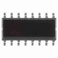
L6566A STMicroelectronics, L6566A Datasheet - Page 18

L6566A
Manufacturer Part Number
L6566A
Description
IC CTRLR OVP UVLO 16SOIC
Manufacturer
STMicroelectronics
Datasheet
1.L6566ATR.pdf
(51 pages)
Specifications of L6566A
Output Isolation
Isolated
Frequency Range
93 ~ 107kHz
Voltage - Input
8 ~ 23 V
Power (watts)
750mW
Operating Temperature
-40°C ~ 150°C
Package / Case
16-SOIC (0.154", 3.90mm Width)
Output Current
800 mA
Output Power
750 mW
Input Voltage
8 V to 23 V
Operating Temperature Range
- 40 C to + 150 C
Mounting Style
SMD/SMT
Duty Cycle (max)
75 %
Universal Input Mains Range
90÷264Vac - Frequency 45 ÷ 65 Hz
Output Voltage
19 V@4 A continuous operation
Mains Harmonics
Acc. to EN61000-3-2 Class-D
St-by Mains Consumption
Less than 0.25 W @265Vac
Overall Efficiency
Better than 86%
Emi
According to EN55022-Class-B
Safety
According to EN60950
Low Profile Design
25 mm maximum height
Pcb Single Layer
single side, 70 μm, CEM-1, 78x174 mm, Mixed PTH/SMT
For Use With
497-8834 - BOARD DEMO FOR L6563/LL6566A497-6452 - BOARD EVAL FOR L6566B497-6451 - BOARD EVAL FOR L6566B497-6450 - BOARD EVAL FOR L6566B497-6449 - BOARD EVAL FOR L6566A
Lead Free Status / RoHS Status
Lead free / RoHS Compliant
Available stocks
Company
Part Number
Manufacturer
Quantity
Price
Company:
Part Number:
L6566A
Manufacturer:
NXP
Quantity:
10 000
Part Number:
L6566A
Manufacturer:
ST
Quantity:
20 000
Part Number:
L6566ATR
Manufacturer:
ST
Quantity:
20 000
Application information
5.1
18/51
If FF operation is selected:
1.
Equation 1
2.
The L6566A is specifically designed for flyback converters operated from front-end power
factor correction (PFC) stages in applications supposed to comply with EN61000-3-2 or
JEITA-MITI regulations. Pin 6 (Vcc_PFC) provides the supply voltage to the PFC control IC.
High-voltage start-up generator
Figure 5
It is made up of a high-voltage N-channel FET, whose gate is biased by a 15 MΩ resistor,
with a temperature-compensated current generator connected to its source.
Figure 5.
FF mode from heavy to light load. The system operates exactly like a standard current
mode, at a frequency f
DCM and CCM transformer operation are possible, depending on whether the power
that it processes is greater or less than:
where Vin is the input voltage to the converter, V
regulated output voltage times the primary-to-secondary turn ratio) and Lp the
inductance of the primary winding. Pin
continuous to discontinuous operation mode of the transformer.
Burst-mode with no or very light load. This kind of operation is activated in the same
way and results in the same behavior as previously described for QR operation.
shows the internal schematic of the high-voltage start-up generator (HV generator).
High-voltage start-up generator: internal schematic
L6566A
Vcc_OK
sw
determined by the externally programmable oscillator: both
Pin
15 M
T
T
CONTROL
=
is the power level that marks the transition from
HV_EN
⎛
⎜ ⎜
⎝
Vin
GND
3
Vin
f 2
sw
+
V
V
1
R
Lp
HV
R
R
I
charge
I
HV
the reflected voltage (i.e. the
⎞
⎟ ⎟
⎠
2
5
Vcc
L6566A


