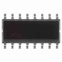
L6566A STMicroelectronics, L6566A Datasheet - Page 25

L6566A
Manufacturer Part Number
L6566A
Description
IC CTRLR OVP UVLO 16SOIC
Manufacturer
STMicroelectronics
Datasheet
1.L6566ATR.pdf
(51 pages)
Specifications of L6566A
Output Isolation
Isolated
Frequency Range
93 ~ 107kHz
Voltage - Input
8 ~ 23 V
Power (watts)
750mW
Operating Temperature
-40°C ~ 150°C
Package / Case
16-SOIC (0.154", 3.90mm Width)
Output Current
800 mA
Output Power
750 mW
Input Voltage
8 V to 23 V
Operating Temperature Range
- 40 C to + 150 C
Mounting Style
SMD/SMT
Duty Cycle (max)
75 %
Universal Input Mains Range
90÷264Vac - Frequency 45 ÷ 65 Hz
Output Voltage
19 V@4 A continuous operation
Mains Harmonics
Acc. to EN61000-3-2 Class-D
St-by Mains Consumption
Less than 0.25 W @265Vac
Overall Efficiency
Better than 86%
Emi
According to EN55022-Class-B
Safety
According to EN60950
Low Profile Design
25 mm maximum height
Pcb Single Layer
single side, 70 μm, CEM-1, 78x174 mm, Mixed PTH/SMT
For Use With
497-8834 - BOARD DEMO FOR L6563/LL6566A497-6452 - BOARD EVAL FOR L6566B497-6451 - BOARD EVAL FOR L6566B497-6450 - BOARD EVAL FOR L6566B497-6449 - BOARD EVAL FOR L6566A
Lead Free Status / RoHS Status
Lead free / RoHS Compliant
Available stocks
Company
Part Number
Manufacturer
Quantity
Price
Company:
Part Number:
L6566A
Manufacturer:
NXP
Quantity:
10 000
Part Number:
L6566A
Manufacturer:
ST
Quantity:
20 000
Part Number:
L6566ATR
Manufacturer:
ST
Quantity:
20 000
L6566A
5.4
Figure 13.
COMP
Figure 12. Addition of an offset to the current sense lowers the burst-mode
Adaptive UVLO
A major problem when optimizing a converter for minimum no-load consumption is that the
voltage generated by the auxiliary winding under these conditions falls considerably as
compared even to a few mA load. This very often causes the supply voltage Vcc of the
control IC to drop and go below the UVLO threshold so that the operation becomes
intermittent, which is undesired. Furthermore, this must be traded off against the need of
generating a voltage not exceeding the maximum allowed by the control IC at full load.
To help the designer overcome this problem, the device, besides reducing its own
consumption during burst-mode operation, also features a proprietary adaptive UVLO
function. It consists of shifting the UVLO threshold downwards at light load, namely when
the voltage at pin COMP falls below a threshold V
Interface"), so as to have more headroom. To prevent any malfunction during transients from
minimum to maximum load the normal (higher) UVLO threshold is re-established when the
voltage at pin COMP exceeds V
Vcc has exceeded the normal UVLO threshold (see
ensures that at full load the MOSFET will be driven with a proper gate-to-source voltage.
Adaptive UVLO block
(*) Vcc
9
V
V
COMPL
COMPO
OFF2
< Vcc
-
+
OFF1
is selected when Q is high
Vcc_PFC
Vcc_PFC
logic
operation threshold
6
R
S
Vcc
Q
OFF1
+
-
Vref
Vcc
L6566A
SW
(*)
OFF2
COMPL
Vcc
10
5
+
-
3
UVLO
L6566A
(see "
7
4
Vcs
o
Chapter 5.8: PFC interface on page 31
= Vref
Vcc_PFC
VCOMP
(pin 6)
(pin 9)
(pin 5)
Vcc
Vcc
V
V
Vcc
Rc
COMPL
COMPO
COMPO
OFF1
OFF2
R + Rc
Q
Figure 13
R
R
internally fixed (see "PFC
Tdelay
). The normal UVLO threshold
Rs
Application information
t
t
t
t
") and
25/51


