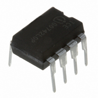
ICE2A265 Infineon Technologies, ICE2A265 Datasheet - Page 11

ICE2A265
Manufacturer Part Number
ICE2A265
Description
IC OFFLINE CTRLR SMPS CM 8DIP
Manufacturer
Infineon Technologies
Series
CoolSET®F2r
Type
Off Line Switcherr
Datasheet
1.ICE2A180Z.pdf
(36 pages)
Specifications of ICE2A265
Package / Case
8-DIP (0.300", 7.62mm)
Output Isolation
Isolated
Frequency Range
93 ~ 107kHz
Voltage - Input
8.5 ~ 22 V
Voltage - Output
650V
Power (watts)
52W
Operating Temperature
-40°C ~ 150°C
Output Voltage
650 V
Input / Supply Voltage (max)
22 V
Input / Supply Voltage (min)
- 0.3 V
Duty Cycle (max)
72 %
Switching Frequency
100 KHz
Supply Current
6.1 mA
Operating Temperature Range
- 40 C to + 150 C
Mounting Style
Through Hole
Maximum Operating Temperature
+ 150 C
Minimum Operating Temperature
- 40 C
Output Power
52 W
Lead Free Status / RoHS Status
Lead free / RoHS Compliant
Lead Free Status / RoHS Status
Lead free / RoHS Compliant, Lead free / RoHS Compliant
Other names
ICE2A265IN
ICE2A265X
ICE2A265XK
ICE2A265XTIN
ICE2A265XTIN
SP000013503
ICE2A265X
ICE2A265XK
ICE2A265XTIN
ICE2A265XTIN
SP000013503
Available stocks
Company
Part Number
Manufacturer
Quantity
Price
Company:
Part Number:
ICE2A265
Manufacturer:
HOLTEK
Quantity:
3 000
Company:
Part Number:
ICE2A265
Manufacturer:
INFINEON
Quantity:
5 510
Part Number:
ICE2A265
Manufacturer:
INFINEON/英飞凌
Quantity:
20 000
Company:
Part Number:
ICE2A265Z
Manufacturer:
INFINEON
Quantity:
570
secondary output voltage is insensitive on line
variations.
waveform slope which controls the duty cycle.
The external R
the maximum source current of the integrated
CoolMOS™.
Figure 9
To improve the Current Mode during light load
conditions the amplified current ramp of the PWM-OP
is superimposed on a voltage ramp, which is built by
the switch T
low pass filter composed of R
Figure 10). Every time the oscillator shuts down for
max. duty cycle limitation the switch T2 is closed by
V
opened so that the voltage ramp can start.
In case of light load the amplified current ramp is to
small to ensure a stable regulation. In that case the
Voltage Ramp is a well defined signal for the
comparison with the FB-signal. The duty cycle is then
controlled by the slope of the Voltage Ramp.
By means of the Comparator C5, the Gate Driver is
switched-off until the voltage ramp exceeds 0.3V. It
allows the duty cycle to be reduced continuously till 0%
by decreasing V
Version 2.6
OSC
Oscillator
FB
. When the oscillator triggers the Gate Driver T2 is
Voltage Ramp
Soft-Start Comparator
V
OSC
Improved Current Mode
2
T
Line
, the voltage source V
2
Sense
C
FB
1
0.3V
below that threshold.
variation
allows an individual adjustment of
10kΩ
R
20pF
1
PWM Comparator
C5
changes
1
0.8V
and C
V
1
Gate Driver
PWM-Latch
1
and the 1st order
1
PWM OP
(see Figure 9,
x3.65
the
current
11
Figure 10
3.2.1
The input of the PWM-OP is applied over the internal
leading edge blanking to the external sense resistor
R
source current into a sense voltage. The sense voltage
is amplified with a gain of 3.65 by PWM OP. The output
of the PWM-OP is connected to the voltage source V1.
The voltage ramp with the superimposed amplified
current signal is fed into the positive inputs of the PWM-
Comparator, C5 and the Soft-Start-Comparator.
3.2.2
The PWM-Comparator compares the sensed current
signal of the integrated CoolMOS
signal V
external
combination with the internal pull-up resistor R
provides the load information of the feedback circuitry.
When the amplified current signal of the integrated
CoolMOS™ exceeds the signal V
Comparator switches off the Gate Driver.
Sense
0.8V
0.3V
Voltage Ramp
Gate Driver
FB
V
connected to pin Isense. R
OSC
FB
optocoupler
PWM-OP
PWM-Comparator
Light Load Conditions
(see Figure 11). V
Duty Cycle
max.
Functional Description
or
external
FB
CoolSET™-F2
TM
Sense
is created by an
with the feedback
FB
25 Dec 2006
transistor
converts the
the PWM-
FB
t
and
t
t
in


