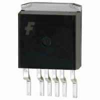
FSCM0465RJ Fairchild Semiconductor, FSCM0465RJ Datasheet - Page 12

FSCM0465RJ
Manufacturer Part Number
FSCM0465RJ
Description
IC SWIT PWM GREEN OVP HV D2PAK
Manufacturer
Fairchild Semiconductor
Datasheet
1.FSCM0465RJX.pdf
(20 pages)
Specifications of FSCM0465RJ
Output Isolation
Isolated
Frequency Range
60 ~ 72kHz
Voltage - Input
8 ~ 20 V
Voltage - Output
650V
Power (watts)
55W
Operating Temperature
25°C ~ 150°C
Package / Case
TO-263-7, D²Pak (6 leads + Tab), TO-263CB
Power Switch Family
FSCM0465R
Input Voltage
85 to 265V
Power Switch On Resistance
2.2Ohm
Output Current
2.3A
Number Of Outputs
Single
Mounting
Surface Mount
Supply Current
2.5mA
Package Type
D2PAK
Operating Temperature (min)
-25C
Operating Temperature (max)
85C
Operating Temperature Classification
Commercial
Pin Count
5 +Tab
Power Dissipation
140W
Lead Free Status / RoHS Status
Lead free / RoHS Compliant
FSCM0465R Rev. 1.0.1
© 2006 Fairchild Semiconductor Corporation
transition. To avoid this undesired operation, the
overload protection circuit is designed to be activated
after a specified time to determine whether it is a
transient situation or an overload situation. Because of
the pulse-by-pulse current limit capability, the maximum
peak current through the SenseFET is limited and the
maximum input power is restricted with a given input
voltage. If the output consumes beyond this maximum
power, the output voltage (V
voltage. This reduces the current through the opto-
coupler LED, which also reduces the opto-coupler
transistor current, increasing the feedback voltage (Vfb).
If Vfb exceeds 2.5V, D1 is blocked and the 5.3µA current
source (I
this condition, Vfb continues increasing until it reaches
6V, when the switching operation is terminated as shown
in Figure 21. The delay time for shutdown is the time
required to charge C
(I
applications.
3.2 Over-Voltage Protection (OVP) : If the secondary-
side feedback circuit were to malfunction or a solder
defect causes an opening in the feedback path, the
current through the opto-coupler transistor becomes
almost zero. In this case, Vfb climbs up in a similar
manner to the overload situation, forcing the preset
maximum current to be supplied to the SMPS until the
overload protection is activated. Because more energy
than required is provided to the output, the output
voltage may exceed the rated voltage before the
overload protection is activated, resulting in the
breakdown of the devices in the secondary side. To
prevent this situation, an over- voltage protection (OVP)
circuit is employed. In general, V
output voltage and the FSCM0465R uses V
directly monitoring the output voltage. If V
19V, an OVP circuit is activated, resulting in the
termination of the switching operation. To avoid
undesired activation of OVP during normal operation,
V
delay
CC
6.0V
2.5V
should be designed to be below 19V.
V
). A 10 ~ 50ms delay time is typical for most
FB
delay
Figure 21. Overload Protection
) starts to charge C
T
1
B
Overload Protection
T
12
from 2.5V to 6.0V with 5.3µA
= C
B
O
*(6.0-2.5)/I
) decreases below the set
CC
B
slowly up to V
is proportional to the
delay
FSCM0465R Rev. 00
CC
CC
T
instead of
2
exceeds
t
CC
. In
12
3.3 Thermal Shutdown (TSD) : The SenseFET and the
control IC are built in one package. This makes it easy
for the control IC to detect the heat generation from the
SenseFET.
approximately 145°C, the thermal protection is triggered,
resulting in shutdown of the FPS.
4. Frequency Modulation : EMI reduction can be
accomplished by modulating the switching frequency of
a switched power supply. Frequency modulation can
reduce EMI by spreading the energy over a wider
frequency range than the bandwidth measured by the
EMI test equipment. The amount of EMI reduction is
directly related to the depth of the reference frequency.
As can be seen in Figure 22, the frequency changes
from 63KHz to 69KHz in 4ms.
5. Soft-Start : The FSCM0465R has an internal soft-start
circuit that increases PWM comparator inverting input
voltage, together with the SenseFET current, slowly after
it starts up. The typical soft-start time is15ms. The pulse
width to the power switching device is progressively
increased to establish the correct working conditions for
transformers, rectifier diodes, and capacitors. The
voltage on the output capacitors is progressively
increased with the intention of smoothly establishing the
required
saturation and reducing stress on the secondary diode
during startup is also helpful.
FSCM0465R Rev. 00
69kHz
66kHz
63kHz
f
s
Drain Current
Figure 22. Frequency Modulation
output
When
T
T
T
s
s
s
voltage.
the
4ms
Preventing
temperature
www.fairchildsemi.com
transformer
t
exceeds


