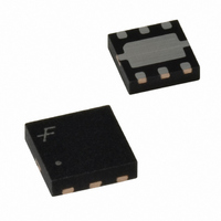
FAN3100CMPX Fairchild Semiconductor, FAN3100CMPX Datasheet - Page 16

FAN3100CMPX
Manufacturer Part Number
FAN3100CMPX
Description
IC GATE DRVR SGL CMOS 2A 6MLP
Manufacturer
Fairchild Semiconductor
Type
Low Sider
Datasheet
1.FAN3100CSX.pdf
(22 pages)
Specifications of FAN3100CMPX
Configuration
Low-Side
Input Type
Differential
Delay Time
15ns
Current - Peak
3A
Number Of Configurations
1
Number Of Outputs
1
Voltage - Supply
4.5 V ~ 18 V
Operating Temperature
-40°C ~ 125°C
Mounting Type
Surface Mount
Package / Case
6-MLP
Rise Time
20 ns
Fall Time
14 ns
Supply Voltage (min)
4.5 V
Supply Current
0.35 mA
Maximum Operating Temperature
+ 125 C
Mounting Style
SMD/SMT
Minimum Operating Temperature
- 40 C
Number Of Drivers
1
Lead Free Status / RoHS Status
Lead free / RoHS Compliant
High Side Voltage - Max (bootstrap)
-
Lead Free Status / Rohs Status
Lead free / RoHS Compliant
Other names
FAN3100CMPXTR
© 2007 Fairchild Semiconductor Corporation
FAN3100 • Rev. 1.0.3
Figure 44 shows the current path when the gate driver
turns the MOSFET off. Ideally, the driver shunts the
current directly to the source of the MOSFET in a small
circuit loop. For fast turn-off times, the resistance and
inductance in this path should be minimized.
Truth Table of Logic Operation
The FAN3100 truth table indicates the operational states
using the dual-input configuration. In a non-inverting
driver configuration, the IN- pin should be a logic low
signal. If the IN- pin is connected to logic high, a disable
function is realized, and the driver output remains low
regardless of the state of the IN+ pin.
In the non-inverting driver configuration in Figure 45, the
IN- pin is tied to ground and the input signal (PWM) is
applied to IN+ pin. The IN- pin can be connected to logic
high to disable the driver and the output remains low,
regardless of the state of the IN+ pin.
In the inverting driver application shown in Figure 46, the
IN+ pin is tied high. Pulling the IN+ pin to GND forces the
output low, regardless of the state of the IN- pin.
Figure 44. Current Path for MOSFET Turn-Off
IN+
0
0
1
1
Figure 45. Dual-Input Driver Enabled,
Figure 46. Dual-Input Driver Enabled,
Non-Inverting Configuration
Inverting Configuration
IN-
0
1
0
1
OUT
0
0
1
0
16
www.fairchildsemi.com


