BTS117 Infineon Technologies, BTS117 Datasheet
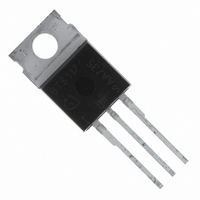
IC LOW SIDE SW PWR 3.5A TO-220-3

BTS117

Manufacturer Part Number
BTS117
Description
IC LOW SIDE SW PWR 3.5A TO-220-3
Manufacturer
Infineon Technologies
Series
HITFET®r
Type
Low Sider
Datasheets

Specifications of BTS117

Input Type
Non-Inverting
Number Of Outputs
1
On-state Resistance
80 mOhm
Current - Output / Channel
3.5A
Current - Peak Output
25A
Voltage - Supply
2.2 V ~ 10 V
Operating Temperature
-40°C ~ 150°C
Mounting Type
Through Hole
Package / Case
TO-220-2
Module Configuration
Low Side
Peak Output Current
3.5A
Output Resistance
0.08ohm
Input Delay
40µs
Output Delay
70µs
Supply Voltage Range
1.3V To 10V
Driver Case Style
TO-220
No. Of Pins
3
Packages
P-TO220-3
Channels
1.0
Vds (max)
60.0 V
Id(nom)
3.5 A
Rds (on) (max)
100.0 mOhm
Id(lim) (min)
7.0 A
Lead Free Status / RoHS Status
Contains lead / RoHS non-compliant
Other names
BTS117IN
BTS117NK
SP000011195

Available stocks

Company
Part Number
Manufacturer
Quantity
Price
Part Number:
BTS117
Manufacturer:
INF
Quantity:
257
Part Number:
BTS117
Manufacturer:
INFINEON/英飞凌
Quantity:
20 000
Part Number:
BTS117 E3045A
Manufacturer:
INFINEON
Quantity:
354
Part Number:
BTS117E3045A
Manufacturer:
NSC
Quantity:
15 562
Part Number:
BTS117TC
Manufacturer:
INFIINION
Quantity:
471
Part Number:
BTS117TC
Manufacturer:
INFINEON/英飞凌
Quantity:
20 000
Part Number:
BTS117TC
0
Smart Lowside Power Switch
Features
Application
General Description
N channel vertical power FET in Smart SIPMOS
nology. Fully protected by embedded protected functions.
Semiconductor Group
Current limitation
Logic Level Input
Input Protection (ESD)
Thermal Shutdown
Overload protection
Short circuit protection
Overvoltage protection
Status feedback with external input resistor
Analog driving possible
All kinds of resistive, inductive and capacitive loads in switching or
µC compatible power switch for 12 V and 24 V DC applications
Replaces electromechanical relays and discrete circuits
linear applications
1
IN
E S D
protection
Overload
limitation
dv/dt
temperature
protection
lim itation
Current
Over-
Overvoltage
protection
Short circuit
Short circuit
Page 1
protection
protection
Product Summary
Drain source voltage
On-state resistance
Current limit
Nominal load current
Clamping energy
chip on chip tech-
HITFET
Source
Drain
L O A D
3
2
V bb
+
HITFET BTS 117
V
R
I
I
E
D(lim)
D(ISO)
DS
DS(on)
AS
13.07.1998
1000
100 m
3.5
60
M
7
V
A
A
mJ

Related parts for BTS117

BTS117 Summary of contents

Page 1

Smart Lowside Power Switch Features Logic Level Input Input Protection (ESD) Thermal Shutdown Overload protection Short circuit protection Overvoltage protection Current limitation Status feedback with external input resistor Analog driving possible Application All kinds of resistive, inductive and capacitive loads ...

Page 2

Maximum Ratings °C unless otherwise specified Parameter Drain source voltage Drain source voltage for short circuit protection Continuous input current 1) -0.2V V 10V IN V < -0. > 10V IN IN Operating temperature ...

Page 3

Electrical Characteristics Parameter at T =25°C, unless otherwise specified j Characteristics Drain source clamp voltage ...+ 150° Off state drain current -40...+150 °C, V ...

Page 4

Electrical Characteristics Parameter at T =25°C, unless otherwise specified j Characteristics Initial peak short circuit current limit Current limit ...

Page 5

Block Diagramm Terms HITFET Input circuit (ESD protection) IN ESD-ZD I Source ESD zener diodes are not designed for DC current > ...

Page 6

Maximum allowable power dissipation P = f(T ) tot c BTS 117 tot On-state resistance 3.5A; V ...

Page 7

Typ. transfer characteristics =12V; T =25° Transient thermal impedance Z = f(t ) thJC P Parameter: D=t ...

Page 8

Application examples: Status signal of thermal shutdown by monitoring input current HITFET µC µ thermal shutdown IN(3) Semiconductor Group Page 8 BTS ...

Page 9

Package and ordering code all dimensions in mm Ordering code: Q67060-S6500-A3 Semiconductor Group Ordering Code: Q67060-S6500-A2 Page 9 BTS 117 13.07.1998 ...

Page 10

Edition 7.97 Published by Siemens AG, Bereich Halbleiter Vetrieb, Werbung, Balanstraße 73, 81541 München © Siemens AG 1997 All Rights Reserved. Attention please! As far as patents or other rights of third parties are concerned, liability is only assumed for ...

Related keywords