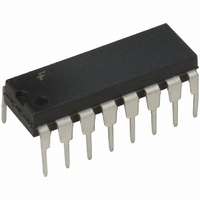
FAN4810N Fairchild Semiconductor, FAN4810N Datasheet - Page 10

FAN4810N
Manufacturer Part Number
FAN4810N
Description
IC PFC CTRLR AVERAGE CURR 16DIP
Manufacturer
Fairchild Semiconductor
Datasheet
1.FAN4810MX.pdf
(14 pages)
Specifications of FAN4810N
Mode
Average Current
Current - Startup
200µA
Voltage - Supply
11 V ~ 16.5 V
Operating Temperature
0°C ~ 70°C
Mounting Type
Through Hole
Package / Case
16-DIP (0.300", 7.62mm)
Switching Frequency
81 KHz
Maximum Operating Temperature
+ 70 C
Mounting Style
Through Hole
Minimum Operating Temperature
0 C
Lead Free Status / RoHS Status
Lead free / RoHS Compliant
Frequency - Switching
-
Lead Free Status / Rohs Status
Lead free / RoHS Compliant
Other names
FAN4810N_NL
FAN4810N_NL
FAN4810N_NL
Available stocks
Company
Part Number
Manufacturer
Quantity
Price
Company:
Part Number:
FAN4810N
Manufacturer:
Fairchild Semiconductor
Quantity:
135
FAN4810
Oscillator (RAMP 1)
The oscillator frequency is determined by the values of RT
and C
oscillator output clock:
The dead time of the oscillator is derived from the following
equation:
at V
The dead time of the oscillator may be determined using:
The dead time is so small (t
operating frequency can typically be approximated by:
EXAMPLE:
For the application circuit shown in the data sheet, with the
oscillator running at:
Solving for R
components values, C
Clock Out (Pin 11)
Clock output is a rail to rail CMOS driver. The PMOS can
pull up within 15 ohms of the rail and the NMOS can pull
down to within 7 ohms of ground.
The clock turns on when the CLKSD pin is greater than
1.25V and the PFC output voltage is at rated operation value.
The clock signal can be used to synchronize and provide on/
off control for downstream DC to DC PWM converters.
CLKSD (Pin 5)
A current source of 25µA supplies the charging current for a
capacitor connected to this pin. Start-up delay can be pro-
grammed by the following equation:
where C
is the desired start-up delay.
10
t
t
C
f
t
f
f
RAMP
DEADTIME
RAMP
OSC
OSC
OSC
dly
REF
T
=
=
=
, which determine the ramp and off-time of the
=
= 7.5V:
dly
=
=
t
--------------- -
t
100kHz
DELAY
--------------------------------------------------- -
t
RAMP
RAMP
C
C
is the required soft start capacitance, and t
1
T
T
T
=
x C
---------------- -
5.5mA
R
R
+
2.5V
T
T
T
t
=
-------------- -
1.25V
25 A
1
DEADTIME
yields 1.96 x 10
--------------- -
t
T
0.51
In
RAMP
= 390pF, and R
1
V
----------------------------- -
V
C
REF
REF
RAMP
T
=
–
–
1.25
3.75
450 C
>> t
-4
DEADTIME
. Selecting standard
T
= 51.1k .
T
) that the
DELAY
(6)
(2)
(3)
(4)
(5)
It is important that the start-up delay is long enough to allow
the PFC time to generate sufficient output power for the
PWM DC converter. The start-up delay should be at least
5ms.
Solving for the minimum value of C
Generating V
The FAN4810 is a voltage-fed part. It requires an external
15V, ±10% (or better) shunt voltage regulator, or some other
V
15V nominal. This allows low power dissipation while at the
same time delivering 13V nominal gate drive at the PFC
OUT output. If using a Zener diode for this function, it is
important to limit the current through the Zener to avoid
overheating or destroying it. This can be easily done with a
single resistor in series with the Vcc pin, returned to a bias
supply of typically 18V to 20V. The resistor’s value must be
chosen to meet the operating current requirement of the
FAN4810 itself (7mA, max.) plus the current required by the
gate driver output and zener diode.
EXAMPLE:
With a V
driving a total gate charge of 38nC at 100kHz (e.g., 1
IRF840 MOSFET ), the gate driver current required is:
Choose R
The FAN4810 should be locally bypassed with a 1.0µF
ceramic capacitor. In most applications, an electrolytic
capacitor of between 47µF and 220µF is also required across
the part, both for filtering and as part of the start-up bootstrap
circuitry.
Typical Applications
Figure 4 is the application circuit for a complete 125W
power factor corrected power supply, designed using the
methods and general topology detailed in Application Note
42046.
C
I
R
R
GATEDRIVE
CC
BIAS
dly
BIAS
regulator, to regulate the voltage supplied to the part at
=
=
=
5ms
BIAS
BIAS
V
---------------------------------
I
------------------------------------------------------ -
7mA
CC
BIAS
CC
of 20V, a V
= 330 .
=
+
-------------- -
1.25V
25 A
20V 15V
+
I
100kHz 38nC
–
G
3.8mA
V
+
CC
–
I
=
Z
CC
100nF
+
of 15V and the FAN4810
5mA
PRODUCT SPECIFICATION
=
=
dly
3.8mA
316
:
REV. 1.0.12 9/24/03
(6a)
(7)
(8)


