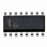
NCP1603D100R2 ON Semiconductor, NCP1603D100R2 Datasheet - Page 16

NCP1603D100R2
Manufacturer Part Number
NCP1603D100R2
Description
IC CTRLR PFC/PWM HV START 16SOIC
Manufacturer
ON Semiconductor
Datasheet
1.NCP1603D100R2.pdf
(30 pages)
Specifications of NCP1603D100R2
Mode
Critical Conduction (CRM), Discontinuous Conduction (DCM)
Frequency - Switching
58kHz
Current - Startup
17µA
Voltage - Supply
9 V ~ 18 V
Operating Temperature
-40°C ~ 125°C
Mounting Type
Surface Mount
Package / Case
16-SOIC (3.9mm Width)
Switching Frequency
405 KHz
Maximum Operating Temperature
+ 125 C
Mounting Style
SMD/SMT
Minimum Operating Temperature
- 40 C
Lead Free Status / RoHS Status
Contains lead / RoHS non-compliant
Other names
NCP1603D100R2OSTR
Introduction
two−stages PFC low−power application.
application circuit is listed in Figure 45. The first−stage PFC
boost circuit draws a near−unity power factor current from the
input but it also steps up the rectified input voltage V
high bulk voltage V
second−stage PWM flyback circuit converts the bulk voltage
V
The controllers of the two stages are combined to become a
single PWM/PFC combo controller. The advantages of
NCP1603 are the following:
(NCP1601 and NCP1230, 100 kHz) The PFC die links up
pin 5 to pin 12 that are in the lower half of Figure 46. The
PWM die links up the other pins that are in the upper half
of Figure 46. For simplicity, the PFC pins are named with
suffix one that stands for the first stage and the PWM pins
are named with suffix two that stands for the second stage.
completely powered off in the standby low−power
condition. It makes the power supply an excellent
low−power no load standby performance.
V
bulk
The NCP1603 is a PWM/PFC combo controller for
NCP1603 is a co−package of two individual IC dies.
This dual−dies architecture allows the PFC die to be
ac
1. Integrated maximum 500 V lossless high voltage
2. Low standby power consumption because of PFC
3. Proprietary PFC methodology limits the
4. Internal ramp compensation for stability
5. Minimum number of external components.
6. Optional synchronization capability between the
7. Safety protection features.
to a usable low voltage and isolated output voltage V
Filter
startup circuit that saves area and power loss.
shutdown and skipping cycle operation.
maximum switching frequency and frequency
jittering feature of the second−stage make the
easier front−ended EMI filter design.
improvement in the second stage converter.
PFC and PWM sections for bulk capacitor ripple
current reduction.
EMI
bulk
V
I
in
L
in the bulk capacitor C
C
R
filter
R
CS1
L
S1
R
I
S
I
FB1
FB1
C
Q
control
Figure 45. Typical Application Circuit
1
D
1
bulk
OPERATING DESCRIPTION
A
NCP1603
. Then, the
http://onsemi.com
typical
in
C
C
C
osc
ramp
to a
bulk
out
.
R
16
FF
Biasing the Controller
operates. The PFC section is the slave section that is
powered off in standby condition for power saving. It is
implemented by connecting V
(Pin 8) together externally. The V
requires a small decoupling external capacitor (0.1 mF) or
nothing. The PWM section powers the PFC section. The
V
PWM section (i.e., V
CC
The PWM section is the master section that always
of the whole device refers to V
V
16
bulk
V
1
bulk
Figure 47. Bias Supply Schematic
GND2
GND1
Figure 46. Internal Connection
V
Out1
14
NCP1603
V
CS2
FB2
Osc
CC1
V
aux
Z
CC2
4
OVP
2
3
4
5
6
7
8
1
6
CC
D
3
R
R
= V
CS2
V
PWM
S2
PFC
8
Die
Die
CC1
CC2
aux
= V
).
aux
pin (Pin 1) and V
Q
I
GND1 = GND2
16
15
14
13 Out2
12
11
10
D
9
C
2
VCC
C
C
D
CC2
HV
NC
V
Ramp
CS1
V
FB1
CC1
out
s
2
CC2
control
(Pin 14) in the
pin generally
Z
CC1
ref
V
out
+
−
pin


