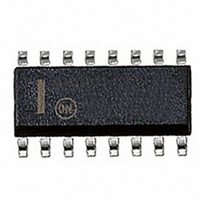
NCP1603D100R2 ON Semiconductor, NCP1603D100R2 Datasheet - Page 21

NCP1603D100R2
Manufacturer Part Number
NCP1603D100R2
Description
IC CTRLR PFC/PWM HV START 16SOIC
Manufacturer
ON Semiconductor
Datasheet
1.NCP1603D100R2.pdf
(30 pages)
Specifications of NCP1603D100R2
Mode
Critical Conduction (CRM), Discontinuous Conduction (DCM)
Frequency - Switching
58kHz
Current - Startup
17µA
Voltage - Supply
9 V ~ 18 V
Operating Temperature
-40°C ~ 125°C
Mounting Type
Surface Mount
Package / Case
16-SOIC (3.9mm Width)
Switching Frequency
405 KHz
Maximum Operating Temperature
+ 125 C
Mounting Style
SMD/SMT
Minimum Operating Temperature
- 40 C
Lead Free Status / RoHS Status
Contains lead / RoHS non-compliant
Other names
NCP1603D100R2OSTR
its timing diagram. When standby condition happens (i.e.,
V
to ensure that the output power remains low for a while.
Then, the V
power saving. The V
goes above 1.25 V immediately because V
possibly above the 0.75 V threshold during standby
operation (referring to Figure 55) and the PFC section is
needed after the circuit restores from standby condition.
diagram of the standby operation respectively. A skipping
cycle behavior of the drain current is made by reset the
latch whenever V
greater than 0.75 V, the duty ratio is modulated by the
PWM block that is illustrated in Figure 50.
V
V
CS2
FB2
I
FB2
CC2
D
FB2
Figure 54 illustrates the standby detection circuitry and
Figure 55 and 56 show the timing diagram and block
Figure 56. Block Diagram in Standby Operation in
Figure 55. Timing Diagram in Standby Condition
< 0.75 V), the controller will wait for a typical 125 ms
2
3
Out2 goes low (no drain current) when V
V
aux
FB2
V
proper operation of the controller and
main output within regulation
CC2
is disabled to shut down the PFC section for
+
−
FB2
needs to be above 7.7 V to ensure
0.75 V
aux
PWM
is smaller than 0.75 V. When V
PWM Section
−
+
(or the PFC) restores when V
Standby
OR
S
R
clock
Q
FB2
Vcc2
FB2
< 0.75 V
can be
time
13
http://onsemi.com
1.25 V
0.75 V
FB2
7.7 V
Out2
FB2
is
21
PFC in Discontinuous/Critical Mode
designed for low−power PFC boost circuit in DCM or CRM
and takes advantages on both operating modes. DCM limits
the maximum switching frequency. It simplifies the
front−ended EMI filter design. CRM limits the maximum
currents of diode, MOSFET and inductor. It reduces the
costs and improves the reliability of the circuit. This device
substantially exhibits unity power factor while operating in
DCM and CRM. It minimizes the number of external
components.
fixed−frequency DCM. In the most stressful conditions,
CRM can be an alternative option that is without power
factor degradation. On the other hand, the PFC section can
be viewed as a CRM controller with a frequency clamp
(maximum switching frequency limit) alternative option
that is also without power factor degradation. In summary,
the PFC section can cover both CRM and DCM without
power factor degradation. Based on the selections of the
boost inductor and the oscillator frequency, the circuit is
capable of the following three applications.
The PFC section of the NCP1603 is NCP1601 that is
The PFC section primarily designed to operate in
1. CRM only by setting the oscillator frequency
2. CRM and DCM by setting the oscillator
3. DCM only by setting the oscillator frequency
V
V
Figure 57. Timing Diagram of the PFC Stage
V
higher than the CRM frequency range.
frequency somewhere within the CRM frequency
range.
lower than the CRM frequency range.
control
ton
current
in
DCM
critical mode
DCM
Inductor current, I
Input current, I
time
time
time
time
L
in


