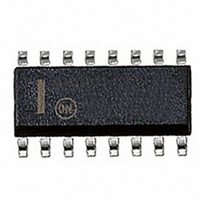
NCP1603D100R2 ON Semiconductor, NCP1603D100R2 Datasheet - Page 20

NCP1603D100R2
Manufacturer Part Number
NCP1603D100R2
Description
IC CTRLR PFC/PWM HV START 16SOIC
Manufacturer
ON Semiconductor
Datasheet
1.NCP1603D100R2.pdf
(30 pages)
Specifications of NCP1603D100R2
Mode
Critical Conduction (CRM), Discontinuous Conduction (DCM)
Frequency - Switching
58kHz
Current - Startup
17µA
Voltage - Supply
9 V ~ 18 V
Operating Temperature
-40°C ~ 125°C
Mounting Type
Surface Mount
Package / Case
16-SOIC (3.9mm Width)
Switching Frequency
405 KHz
Maximum Operating Temperature
+ 125 C
Mounting Style
SMD/SMT
Minimum Operating Temperature
- 40 C
Lead Free Status / RoHS Status
Contains lead / RoHS non-compliant
Other names
NCP1603D100R2OSTR
second−stage drain current I
drops because output voltage collapses. When V
below V
disappears and the V
voltage V
current source activates and charge up the V
reaches V
soft−start activates after V
typical). The peak drain current follows its 2.5 ms
envelope. The power supply dissipates some power due to
the switching signal of Out2 and waits for possible
auto−recovery of operation when the fault is cleared.
feature that allows the drain current in every two V
hiccup cycle in fault condition. The “double hiccup”
feature offers fewer power dissipation during fault
condition comparing to “single hiccup”.
above V
operation. Otherwise, the V
12.6−7.7−5.6−12.6 V hiccup mode until the fault or bulk
voltage is cleared.
Standby Condition
condition and the V
maximum of V
threshold. Hence, the standby threshold is V
3.0 V = 0.75 V.
Figure 53 illustrates the timing diagram of V
As shown in Figure 53, NCP1603 has a “double hiccup”
If the fault is cleared (V
The output voltage rises up excessively in standby
CC2(off)
CC(off)
CC
CC(on)
drops to V
FB2
(7.7 V typical), the Drive Output signal
(7.7 V typical), the circuit will resume its
(12.6 V typical). The internal 2.5 ms
(i.e., 3.0 V) is defined to be the standby
FB2
CC
CC(latch)
drops. A set point of 25% of the
FB2
continues to drop. When bias
12.6 V
Startup current source
charging the V
7.7 V
5.6 V
V
D
CC
CC2
0A
< 3.0 V
I
in fault condition. The V
D
(5.6 V typical), the startup
reaches V
CC
Figure 53. Timing Diagram of Fault Condition
SS
will continue this
) and V
CC
capacitor
Switching starts when
V
CC(on)
CC2
Peak drain current follows
a 2.5 ms soft−start envelope
CC
stby
CC2
CC
Startup circuit turns on
when V
reaches 12.6 V
until V
CC
= 25% ×
(12.6 V
remains
and the
http://onsemi.com
drops
Startup circuit turns off
when V
CC2
CC
CC
CC
is 5.6 V
CC2
20
is 12.6 V
FB2
below 0.75 V and cannot go
1.25 V
0.75 V
Switching is missing
in every two V
featuring a “double hiccup”
V
Figure 54. Block Diagram and Timing Diagram of
above 1.25 V for 125 ms
aux
2
Maximum drain current
is limited to 1 / R
stops when V
0.75 V / 1.25 V
V
V
V FB2
aux
Circuit sleeps when
V
FB2
CC2
CC
125 ms
is below 7.7 V
hiccup cycles
−
+
Standby Detection
FB2
CS2
is
time
125 ms
delay
V
FB2
V
goes above 1.25 V
aux
enable Vaux /
PFC Section
Leave standby
restores when
&
Standby
disable
Vaux/
PFC
Section
time
time


