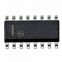
NCP1603D100R2 ON Semiconductor, NCP1603D100R2 Datasheet - Page 18

NCP1603D100R2
Manufacturer Part Number
NCP1603D100R2
Description
IC CTRLR PFC/PWM HV START 16SOIC
Manufacturer
ON Semiconductor
Datasheet
1.NCP1603D100R2.pdf
(30 pages)
Specifications of NCP1603D100R2
Mode
Critical Conduction (CRM), Discontinuous Conduction (DCM)
Frequency - Switching
58kHz
Current - Startup
17µA
Voltage - Supply
9 V ~ 18 V
Operating Temperature
-40°C ~ 125°C
Mounting Type
Surface Mount
Package / Case
16-SOIC (3.9mm Width)
Switching Frequency
405 KHz
Maximum Operating Temperature
+ 125 C
Mounting Style
SMD/SMT
Minimum Operating Temperature
- 40 C
Lead Free Status / RoHS Status
Contains lead / RoHS non-compliant
Other names
NCP1603D100R2OSTR
typical) and the maximum allowable limit is 18 V. On the
other hand, the V
(7.7 V typical). Hence, there are two possible operating
regions in Figure 49. In the non−usable region the V
not high enough to turn on the PFC section. Therefore, the
flyback transformer auxiliary winding must be between
V
200 ns Leading Edge Blanking (LEB) that is to prevent a
premature reset of the output due to noise, a pair of sense
resistors R
I
compensation for a stability improvement to the
current−mode control possibly in continuous mode
operation.
pair of resistors (55 kW and 25 kW). The soft−start
processing circuit reduces the initial voltage−loop
feedback signal (V
soft−start disappears. As a result, the startup envelope of
the peak drain current (or duty ratio) ramps up gradually for
2.5 ms. It is noted that the 2.5 ms is counted when the PWM
die circuit is reset that is when V
(12.6 V typical). This soft−start feature offers a reduced
D
CC1(on)
The UVLO start thresholds of V
The current−loop feedback circuit consists of a typical
The V
, and a 0−to−2.3 V jittering ramp that adds a ramp
V
out
FB2
Opto
Coupler
(10.5 V typical) and 18 V.
CS2
is approximately divided by 3 by an internal
and R
aux
FB2
FB2
is enabled when V
S2
2
/ 3) for 2.5 ms. After this 2.5 ms, the
that sense the flyback drain current
Figure 50. Block Diagram of Duty Cycle Regulation in the PWM Section
Vdd
V
20 k
55 k
25 k
FB2
CC1
CC2
V
FB2
CC2
3
Processing
is V
Soft−Start
Jittering Ramp
Circuit
reaches V
200 ns
is over V
CC1(on)
100 kHz
LEB
18 k
2.3 V
0 V
(10.5 V
CC2(off)
CC2(on)
http://onsemi.com
aux
PWM
is
-
+
6.4% Frequency
Soft−Start Period 2.5 ms
18
Modulation
Jittering
V
Regulation in the PWM Section
is NCP1230 that is a current−mode fixed−frequency PWM
flyback controller with internal compensation ramp. The
simplified block diagram of the duty cycle regulation
section is in Figure 50. A 100 kHz clock oscillator is
modulated by adding a frequency jittering feature. This
modulated 100 kHz clock signal turns the Out2 (pin 13)
high in each switching cycle. The Out2 goes low when the
current−loop feedback signal intersects with the output
voltage−loop feedback signal. A duty cycle is therefore
generated. The maximum duty ratio is limited to D
(80% typical).
transient voltage and current stress on the power circuit
during the startup.
current. It pulls down the V
generates a lower duty ratio. The output voltage reduces.
Insufficient output voltage reduces the optocoupler
current. If the current is too small, the V
pulled high than 3.0 V (3.8 V typical). The (V
is then clamped to an internal 1.0 V limit. If the ramp is
ignored (i.e., R
is derived as:
the ramp getting compared for the modulation. Hence, a
large value of the R
possible maximum duty ratio.
FB2
3
The PWM section (or the second stage) of the NCP1603
Excessive output voltage causes more the optocoupler
It is noted that resistor R
R
S
Max Duty
= 80%
Q
Oscillator
100 kHz
S2
1 V Max
= 0), the maximum possible drain current
S2
V
I D(max) +
CC2
increase the ramp and will reduce the
13
3
FB2
S2
Out2
CS2
will affect the percentage of
through FB2 pin (Pin 2) and
R CS2
R
1 V
S2
V
bulk
R
FB2
CS2
Flyback
Drain
Current
I
D
FB2
is eventually
/3) signal
(eq. 2)
max


