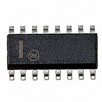
NCP1603D100R2 ON Semiconductor, NCP1603D100R2 Datasheet - Page 26

NCP1603D100R2
Manufacturer Part Number
NCP1603D100R2
Description
IC CTRLR PFC/PWM HV START 16SOIC
Manufacturer
ON Semiconductor
Datasheet
1.NCP1603D100R2.pdf
(30 pages)
Specifications of NCP1603D100R2
Mode
Critical Conduction (CRM), Discontinuous Conduction (DCM)
Frequency - Switching
58kHz
Current - Startup
17µA
Voltage - Supply
9 V ~ 18 V
Operating Temperature
-40°C ~ 125°C
Mounting Type
Surface Mount
Package / Case
16-SOIC (3.9mm Width)
Switching Frequency
405 KHz
Maximum Operating Temperature
+ 125 C
Mounting Style
SMD/SMT
Minimum Operating Temperature
- 40 C
Lead Free Status / RoHS Status
Contains lead / RoHS non-compliant
Other names
NCP1603D100R2OSTR
CRM. In order to keep the operation in DCM and CRM
only, the Drive Output cannot turn on as long as there is
some inductor current flowing through the circuit. Hence,
the zero current signal is provided to the oscillator/
synchronization block in Figure 67. An input comparator
monitors the Osc pin (Pin 5) voltage and generates a clock
signal. The negative edge of the clock signal is stored in a
RS latch. When zero current is detected, the RS latch will
be reset and a set signal is sent to the output drive latch that
turns on the MOSFET in the PFC boost circuit. Figure 68
illustrates a typical timing diagram of the oscillator block.
Oscillator Mode in PFC Section
external capacitor C
V
= 49 mA typical) and the external capacitor C
When the voltage reaches V
sources a current I
capacitor C
300 ns propagation delay and the 3.5 V and 5.0 V threshold
conditions are measured on 220 pF C
actual oscillator hysteresis is a little bit smaller.
in the oscillator pin and the oscillator frequency is to
f
Hence, the oscillator switching frequency can be
formulated in Equation 25 and represented in Figure 70.
Drive output
(latch set signal)
Clock edge
osc(max)
Osc clock
sync(H)
The PFC section is designed to operate in either DCM or
In oscillator mode, the Osc pin (Pin 5) is connected to an
There is an internal capacitance C
Figure 69. Oscillator Mode Timing Diagram in DCM
Osc pin
voltage
(DCM)
(latch output)
clock edge
clock latch
Figure 68. Oscillator Block Timing Diagram
Discontinuous mode
inductor
(5.0 V typical), the pin sinks a current I
current
C osc +
(405 kHz typical) when the Osc pin is opened.
clock
osc
is charged. It is noted that there is a typical
36 pF @ 405 kHz
osc
och
. When the voltage of this pin is above
f osc
(45 mA typical) and the external
sync(L)
Critical mode
* 36 pF
osc
(3.5 V typical), the pin
osc(int)
capacitor. Hence, the
(36 pF typical)
osc
odch
discharges.
(eq. 25)
(94–45
http://onsemi.com
3.5 V
5 V
time
26
Synchronization Option
external digital signal with level high defined to be higher
than V
lower than V
Zener diode is connected to the Osc pin and hence the
maximum allowable synchronization voltage is 9.0 V. The
circuit recognizes a synchronization frequency by the time
difference between two falling edge instants when the
synchronization signal across the 3.5 V threshold point.
The actual synchronization threshold point is a little bit
higher than the 3.5 V threshold point. The minimum
synchronization pulse width is 500 ns.
synchronization threshold point to the moment of output goes
high and there is also a typical 300 ns propagation delay from
the synchronization threshold point to the moment of crossing
3.5 V. Hence, the output goes high apparently when the sync
signal turns to 3.5 V. A timing diagram of synchronization
mode is summarized in Figure 71.
together in order to minimize some of the ripple current in
the bulk capacitor as shown in Figure 72 and 73. The Out2
pin (Pin 13) is the external synchronization signal in
Figure 71 to the PFC Section. When the Out2 is in high
state, the voltage is potentially higher than the maximum
allowable voltage in Osc pin (Pin 5). Hence, a pair of
resistors divides the voltage from Out2 reduces the voltage
Drive Output
Sync Signal
Clock Edge
Osc Clock
Figure 71. Synchronization Mode Timing Diagram in
In synchronization mode, the Osc pin (Pin 5) receives an
There is a typical 350 ns propagation delay from
The PWM and PFC Section can be synchronized
(DCM)
700
600
500
400
300
200
100
0
0
sync(H)
Figure 70. Osc Pin Frequency Setting
sync(L)
(5.0 V typical) and level low defined to be
f
50
osc
(3.5 V typical). An internal 9.0 V ESD
, Oscillator Frequency (kHz)
DCM
100
150
3.5 V
5 V
200


