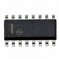
NCP1603D100R2 ON Semiconductor, NCP1603D100R2 Datasheet - Page 17

NCP1603D100R2
Manufacturer Part Number
NCP1603D100R2
Description
IC CTRLR PFC/PWM HV START 16SOIC
Manufacturer
ON Semiconductor
Datasheet
1.NCP1603D100R2.pdf
(30 pages)
Specifications of NCP1603D100R2
Mode
Critical Conduction (CRM), Discontinuous Conduction (DCM)
Frequency - Switching
58kHz
Current - Startup
17µA
Voltage - Supply
9 V ~ 18 V
Operating Temperature
-40°C ~ 125°C
Mounting Type
Surface Mount
Package / Case
16-SOIC (3.9mm Width)
Switching Frequency
405 KHz
Maximum Operating Temperature
+ 125 C
Mounting Style
SMD/SMT
Minimum Operating Temperature
- 40 C
Lead Free Status / RoHS Status
Contains lead / RoHS non-compliant
Other names
NCP1603D100R2OSTR
Figure 47 while a typical completed application schematic
can be referred to Figure 45. These two dies have their own
individual supply voltages at Pin 8 and Pin 14. The grounds
of the two dies are physically connected through the package
substrate but they are needed to be connected externally. The
bias voltage to the NCP1603 comes from the bulk voltage
V
startup, a second−stage flyback transformer auxiliary winding
delivers the supply voltage to V
Lossless High Voltage Startup Circuit
that this pin can be directly connected to the bulk voltage
V
Figure 48 illustrates the block diagram of the startup circuit.
An UVLO comparator monitors the V
current source is activated and deactivated whenever the
voltage reaches V
(12.6 V typical) thresholds respectively. Therefore, the V
never drops below V
circuit is unplugged (i.e., V
minimum required operating threshold V
typical)). This feature makes the controller memorize the
external latch off function implemented in Pin 3.
external components and Printed Circuit Board (PCB) area.
It also minimizes the loss due to startup resistor because
startup resistor always dissipates power but this startup circuit
can be turned off when the V
there is a small leakage current I
HV = 700 V) when the startup circuit is off.
ensure that V
voltage V
bulk
bulk
The recommended biasing schematic of the controller is in
The HV pin (Pin 16) is capable of the maximum 500 V so
This in−chip startup circuit can minimize the number of
The V
Turn on Internal Bias
and delivers startup supply voltage to the controller.
through the HV pin (Pin 16) during startup. After
CC
Counter
CC2(off)
capacitor is recommended to be at least 47 mF to
Double
Hiccup
B2
&
Q S
Figure 48. V
CC
R
is always above the minimum operating
(7.7 V typical) in the startup phase. For
CC2(latch)
Turn Off
CC2(latch)
UVLO
CC2
bulk
CC
3.2 mA
(5.6 V typical) and V
12.6/
5.6 V
20 V
-
+
+
-
after powering up unless the
voltage is sufficient. Actually,
disappears or smaller than its
7.7 V
Management
CC
.
HV3
CC
14
16
at Pin 14. A startup
(30 mA typical at
V
HV
CC
start(min)
V
bulk
http://onsemi.com
CC2(on)
(20 V
CC
17
example, the PWM die consumes I
a 47 mF V
105 ms. It is the available time to establish a V
from the flyback transformer auxiliary winding.
V
powered off during the standby condition where the
low−frequency ripple of V
startup phase since V
V
whatever reason, the PWM section sleeps and it consumes
I
(5.6 V typical). When V
typical), the startup current source activates and V
again.
Auxiliary Supply V
externally. Internally, the V
through an internal MOSFET. The MOSFET on−resistance
is R
the PWM section to the PFC section. The V
when one of the following conditions occurs.
0.75 V
CC2(latch)
t startup +
3.0 V
CC2
CC1
A large enough V
The PFC section does not consume any current in the
When V
The V
aux
1. V
2. Fault condition (V
3. Standby condition (V
4. Insufficient operating supply voltage (V
5. Overvoltage protection (OVP) latch activated from
6. Thermal shutdown latch in the PWM section
= 0 V).
always above V
signal (V
125 ms).
and then V
more than 125 ms).
V
CS2 pin (Pin 3) (V
activated when the junction temperature is over
typical 150_C.
(11.7 W typical). It delivers a supply voltage from
aux
aux
CC2(off)
CC
(680 mA typical) until V
V
CC2
I CC2(op2)
Figure 49. V
C VCC DV
FB2
pin (Pin 1) connects to the V
is initially disabled because of no feedback
capacitor can maintain the V
falls below V
Standby Condition (V
FB2
7.7 V
(7.7 V typical)).
Fault Condition (V
FB2
Enabled
Region
9.0 V
usable
aux
Non−
CC
Vaux
> 3.0 V) initially.
CC2(off)
aux
+
< V
capacitor can also help to maintain
aux
10.5 V
47 mF·(12.6 V−7.7 V)
CC2
is disabled initially (i.e., V
CS2
CC2
FB2
stby−out
12.6 V
Enabled Regions
aux
FB2
to prevent the IC accidentally
> V
can be very high.
> 3.0 V for more than
CC2(off)
reaches V
pin is connected to V
2.2 mA
Enabled
< V
Usable
Region
CC2(op2)
OVP
FB2
(1.25 V typical) for
Vaux
CC2
FB2
> 3.0 V)
stby
(3.0 V typical)).
< 0.75 V)
(7.7 V typical) for
reaches V
CC
(0.75 V typical)
(2.2 mA typical),
CC2(latch)
CC1
18 V
18 V
above 7.7 V for
aux
+ 105 ms
V
V
pin (Pin 8)
is disabled
CC
CC2
CC2
CC1
CC2(latch)
CC2
voltage
(eq. 1)
(PWM)
(PFC)
(5.6 V
<
aux
rises
CC2
=


