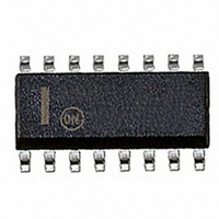
NCP1603D100R2 ON Semiconductor, NCP1603D100R2 Datasheet - Page 4

NCP1603D100R2
Manufacturer Part Number
NCP1603D100R2
Description
IC CTRLR PFC/PWM HV START 16SOIC
Manufacturer
ON Semiconductor
Datasheet
1.NCP1603D100R2.pdf
(30 pages)
Specifications of NCP1603D100R2
Mode
Critical Conduction (CRM), Discontinuous Conduction (DCM)
Frequency - Switching
58kHz
Current - Startup
17µA
Voltage - Supply
9 V ~ 18 V
Operating Temperature
-40°C ~ 125°C
Mounting Type
Surface Mount
Package / Case
16-SOIC (3.9mm Width)
Switching Frequency
405 KHz
Maximum Operating Temperature
+ 125 C
Mounting Style
SMD/SMT
Minimum Operating Temperature
- 40 C
Lead Free Status / RoHS Status
Contains lead / RoHS non-compliant
Other names
NCP1603D100R2OSTR
PIN FUNCTION DESCRIPTION
Pin
10
12
13
14
15
16
11
1
2
3
4
5
6
7
8
9
Symbol
V
GND2
GND1
Ramp
Out1
V
Out2
V
V
FB2
CS2
Osc
FB1
control
CS1
NC
HV
CC1
CC2
aux
PWM Supply Voltage
PWM Current Sense
PFC Control Voltage
PFC Supply Voltage
PFC Current Sense
PWM Drive Output
PFC Drive Output
Auxiliary Supply
PWM Feedback
PFC Feedback
PFC Oscillator
No Connected
PWM Ground
PFC Ground
High Voltage
PFC Ramp
Function
This pin connects to the V
PFC section. The V
(1) V
(2) Fault (V
(3) Standby (V
(4) Overvoltage protection latch activated from CS2 pin;
(5) Thermal shutdown latch in the PWM section;
(6) Insufficient supply voltage (V
The transistor turns on (or V
window (0.75 V < V
An external optocoupler collector pulls the voltage of this pin V
output voltage. The PWM regulation window between V
V
When no feedback signal is received from the optocoupler, V
higher than 3.0 V. If this condition lasts for longer than 125 ms, the controller enters
double−hiccup fault condition.
This pin cumulates three different functions: current−mode PWM regulation, primary
overcurrent protection and overvoltage protection (OVP). If the voltage of this pin is above
3.0 V for OVP, the circuit is latched off until V
An external noise decoupling pF−order capacitor is connected to the pin to prevent the latch
protection activated due to noise.
−
In oscillator mode, this pin is connected to an external capacitor to set the oscillator
frequency in DCM operation. In synchronization mode, this pin is connected to an external
driving signal. However, if the PFC−stage inductor current is non−zero at the end of a
switching period, the PFC−stage circuit will be forced to CRM and the Out1 is out of
synchronization to the Osc pin signal.
−
This pin provides an output to an external MOSFET in the PFC section.
This pin is the positive supply of the PFC section. the operating range is between 9.0 V and
18 V with UVLO start threshold 10.5 V.
This pin receives a current I
for the output regulation, PFC section overvoltage protection (OVP) and PFC section output
undervoltage protection (UVP). When I
Drive Output is disabled. When I
low−current consumption shutdown mode.
The control voltage V
of the circuit. This pin is connected to an external capacitor to limit the control voltage
bandwidth typically below 20 Hz to achieve Power Factor Correction purpose.
This pin receives a current I
overcurrent protection (OCP), and zero current detection. When I
is activated and the Drive Output (Out1) is disabled. When I
recognized to be a zero current for feedback regulation and DCM or CRM operation in the
PFC oscillator section.
This pin is connected to an external capacitor to set a ramp signal. The capacitor value
directly affects the input impedance of the PFC circuit and its maximum input power.
This pin provides an output to an external MOSFET in the PWM section.
This pin is basically the positive supply of the PWM section. It is also the positive supply of
the whole device because the PFC section is also supplied from this pin indirectly through
V
V
This pin is for high voltage clearance of the HV pin.
This pin connects to the bulk DC voltage to deliver power to the controller in startup or fault
condition. The internal startup circuit is disabled in normal and standby condition for power
saving purpose. The UVLO stop and start thresholds of the startup circuit are V
and V
aux
FB2
CC2
aux
pin (Pin 1). The operating range is between 7.7 V and 18 V. The circuit resets when
drops below 0.75 V, the controller enters standby operation.
drops below 4.0 V.
CC2
is initially off;
= 5.6 V.
FB2
http://onsemi.com
FB2
> 3.0 V for more than 125 ms);
< 0.75 V and then V
aux
FB2
control
4
is disabled when either one of the following conditions occurs:
< 3.0 V).
CC1
directly controls the input impedance and hence the power factor
FB1
S
aux
that is proportional to the inductor current. The current is for
pin externally. It delivers a bias voltage from the V
is enabled) when V
that represents the PFC circuit output voltage. The current is
CC2
FB1
< 7.7 V).
goes below 14 mA, the PFC section enters a
FB2
FB1
Description
is smaller than 1.25 V for more than 125 ms);
goes above 107% I
CC2
resets. The PWM Drive Output is disabled.
FB2
is within the normal mode regulation
FB2
= 0.75 V and V
S
FB2
goes below 14 mA, it is
ref
FB2
, OVP is activated and the
is internally pulled to be
S
down to regulate the
goes above 200 mA, OCP
FB2
= 3.0 V. When
CC2
CC2
= 12.6 V
to the


