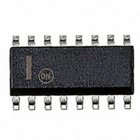
NCP1603D100R2 ON Semiconductor, NCP1603D100R2 Datasheet - Page 28

NCP1603D100R2
Manufacturer Part Number
NCP1603D100R2
Description
IC CTRLR PFC/PWM HV START 16SOIC
Manufacturer
ON Semiconductor
Datasheet
1.NCP1603D100R2.pdf
(30 pages)
Specifications of NCP1603D100R2
Mode
Critical Conduction (CRM), Discontinuous Conduction (DCM)
Frequency - Switching
58kHz
Current - Startup
17µA
Voltage - Supply
9 V ~ 18 V
Operating Temperature
-40°C ~ 125°C
Mounting Type
Surface Mount
Package / Case
16-SOIC (3.9mm Width)
Switching Frequency
405 KHz
Maximum Operating Temperature
+ 125 C
Mounting Style
SMD/SMT
Minimum Operating Temperature
- 40 C
Lead Free Status / RoHS Status
Contains lead / RoHS non-compliant
Other names
NCP1603D100R2OSTR
protection function, it is generaly recommended to put a
pF−order decoupling ceramic capacitor across the CS2 pin
to remove possible high−frequency noise there.
configured in Figure 74. A PNP bipolar transistor is added
to open the Zener diode Z
to stop any interference of the normal operation of current
sense. It is because the Zener diode easily pulls high the
CS2 pin voltage to 1.0 V and that interferes with the normal
operation of the current sense when the output is high. The
OVP threshold V
(6) Latched Overvoltage Protection (OVP)
not affect the normal regulation operation of current sense,
the protection can be implemented. An alternative is to
implement the output overvoltage protection by an
optocoupler in Figure 75. The leakage current of the added
circuit is up to the zener diode at the output voltage. When
there is no overvoltage, the leakage is small and it does not
affect the normal operation. A resistor paralleled to the
optocoupler is added to share the potential increasing
In order to prevent wrongly triggering the latch
To set the V
As long as an external protection on CS2 pin (Pin 3) does
Figure 74. V
CS2
V CC2(OVP) + V ZOVP ) 3 V
CC
CC
CC2(OVP)
overvoltage protection, the circuit is
Latched OVP Application Circuit
V
OVP
CC2
is expressed in Equation 26.
Z
OVP
when Out2 is high in order
R
R
S2
CS2
(eq. 26)
http://onsemi.com
28
leakage current of the zener diode due to temperature
variation. The Zener diode at the output voltage is
recommended to be a 1 mA operating current at the
threshold voltage. Then, this current is coupled through the
optocoupler and inserts a similar order of current
(depending on the current−transfer−ratio CTR of the
optocoupler) into CS2 pin. The CS2 pin is capable of up to
100 mA and with an internal 9 V anti−parallel ESD diode
but it is recommended to put a 8.2 V Zener diode there to
further protect the pin.
(7) Dual Thermal Shutdown (TSD)
incorporates their individual thermal shutdown. The PFC
thermal circuitry disables the PFC gate drive Out1 and then
keeps the power switch off when its junction temperature
exceeds 170 °C typically. The PFC gate drive Out1 is then
enabled once the temperature drops below typically 125°C
(i.e., 45°C hysteresis).
Out2 and then keeps the power switch off when its junction
temperature exceeds 165°C typically. The PWM gate drive
Out2 is then enabled once the temperature drops below
typically 140°C and the circuit is unplugged (to make V
drops below 4.0 V).
The NCP1603 consists of two individual dies that
The PWM thermal circuitry disables the PWM gate drive
Figure 75. Output Latched OVP Application Circuit
CS2
V
CC2
V
out
Z
OVP
R
R
S2
CS2
CC2


