C8051T610DB28 Silicon Laboratories Inc, C8051T610DB28 Datasheet - Page 126
C8051T610DB28
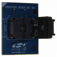
Manufacturer Part Number
C8051T610DB28
Description
DAUGHTER BOARD T610 28QFN SOCKET
Manufacturer
Silicon Laboratories Inc
Datasheet
1.C8051T610DB32.pdf
(218 pages)
Specifications of C8051T610DB28
Module/board Type
Socket Module - QFN
Processor To Be Evaluated
C8051T61x
Interface Type
USB
Lead Free Status / RoHS Status
Lead free / RoHS Compliant
For Use With/related Products
C8051T610DK
Lead Free Status / RoHS Status
Lead free / RoHS Compliant, Lead free / RoHS Compliant
Other names
336-1506


C8051T610/1/2/3/4/5/6/7
SFR Definition 21.6. P0SKIP: Port 0 Skip
SFR Address = 0xD4
SFR Definition 21.7. P1: Port 1
SFR Address = 0x90; Bit-Addressable
126
Note: P1.6 and P1.7 are not connected to external pins on the C8051T616/7 devices.
Name
Reset
Name
Reset
7:0
7:0
Bit
Bit
Type
Type
Bit
Bit
P0SKIP[7:0]
P1[7:0]
Name
Name
7
0
7
1
Port 1 Data.
Sets the Port latch logic
value or reads the Port pin
logic state in Port cells con-
figured for digital I/O.
Port 0 Crossbar Skip Enable Bits.
These bits select Port 0 pins to be skipped by the Crossbar Decoder. Port pins
used for analog, special functions or GPIO should be skipped by the Crossbar.
0: Corresponding P0.n pin is not skipped by the Crossbar.
1: Corresponding P0.n pin is skipped by the Crossbar.
6
0
6
1
Description
5
0
5
1
0: Set output latch to logic
LOW.
1: Set output latch to logic
HIGH.
Rev 1.0
4
0
4
1
P0SKIP[7:0]
P1[7:0]
R/W
R/W
Function
Write
3
0
3
1
2
0
2
1
0: P1.n Port pin is logic
LOW.
1: P1.n Port pin is logic
HIGH.
1
0
1
1
Read
0
0
0
1
Related parts for C8051T610DB28
Image
Part Number
Description
Manufacturer
Datasheet
Request
R

Part Number:
Description:
SMD/C°/SINGLE-ENDED OUTPUT SILICON OSCILLATOR
Manufacturer:
Silicon Laboratories Inc
Part Number:
Description:
Manufacturer:
Silicon Laboratories Inc
Datasheet:
Part Number:
Description:
N/A N/A/SI4010 AES KEYFOB DEMO WITH LCD RX
Manufacturer:
Silicon Laboratories Inc
Datasheet:
Part Number:
Description:
N/A N/A/SI4010 SIMPLIFIED KEY FOB DEMO WITH LED RX
Manufacturer:
Silicon Laboratories Inc
Datasheet:
Part Number:
Description:
N/A/-40 TO 85 OC/EZLINK MODULE; F930/4432 HIGH BAND (REV E/B1)
Manufacturer:
Silicon Laboratories Inc
Part Number:
Description:
EZLink Module; F930/4432 Low Band (rev e/B1)
Manufacturer:
Silicon Laboratories Inc
Part Number:
Description:
I°/4460 10 DBM RADIO TEST CARD 434 MHZ
Manufacturer:
Silicon Laboratories Inc
Part Number:
Description:
I°/4461 14 DBM RADIO TEST CARD 868 MHZ
Manufacturer:
Silicon Laboratories Inc
Part Number:
Description:
I°/4463 20 DBM RFSWITCH RADIO TEST CARD 460 MHZ
Manufacturer:
Silicon Laboratories Inc
Part Number:
Description:
I°/4463 20 DBM RADIO TEST CARD 868 MHZ
Manufacturer:
Silicon Laboratories Inc
Part Number:
Description:
I°/4463 27 DBM RADIO TEST CARD 868 MHZ
Manufacturer:
Silicon Laboratories Inc
Part Number:
Description:
I°/4463 SKYWORKS 30 DBM RADIO TEST CARD 915 MHZ
Manufacturer:
Silicon Laboratories Inc
Part Number:
Description:
N/A N/A/-40 TO 85 OC/4463 RFMD 30 DBM RADIO TEST CARD 915 MHZ
Manufacturer:
Silicon Laboratories Inc
Part Number:
Description:
I°/4463 20 DBM RADIO TEST CARD 169 MHZ
Manufacturer:
Silicon Laboratories Inc