OM6277,598 NXP Semiconductors, OM6277,598 Datasheet - Page 11
OM6277,598
Manufacturer Part Number
OM6277,598
Description
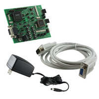
DEMO BOARD FOR PCA9564
Manufacturer
NXP Semiconductors
Datasheet
1.OM6277598.pdf
(52 pages)
Specifications of OM6277,598
Main Purpose
Interface, I2C Controller
Embedded
Yes, MCU, 8-Bit
Utilized Ic / Part
PCA9564
Primary Attributes
I2C Bus Controller, 1 8-Bit GPIO, 1 8-Bit LED Dimmer
Secondary Attributes
8 Momentary Switches, 23 LEDs
Lead Free Status / RoHS Status
Not applicable / Not applicable
Other names
568-4001
935283226598
935283226598


Miscellaneous
•
•
•
•
externally supplied and is limited to 5.5 V.
P89LV51 RxD pin can be connected to the P89LPC932 TxD pin through jumper JP18
-
-
Note:
Jumpers JP2 and JP3 must be open when JP17 and JP18 need to be closed.
Power supply for daughter cards connected to the I
Jumper JP8 (VDD Conn), when closed, connect the V
internal 3.3 V regulated voltage, thus allowing daughter cards to be supplied directly by the main board
-
-
General purpose LEDs:
Several LEDs are connected to the P89LV51RD2 and the P89LPC932 for debugging or general-purpose use.
LD1 to LD8 are accessible by both microcontrollers through I
General Purpose jumpers for P89LPC932:
Jumpers JP19, JP20 and JP21 allows to force HIGH or LOW logic levels respectively on pins P0.0, P0.1 and P0.2
of the P89LPC932.
-
-
General purpose headers for both microcontrollers:
PORT1LV51 and PORT0LPC headers allow to easily access to Port 0 of each device for monitoring or external
control. V
Note:
Header labeled “3v3” on PORT0LV51 is actually connected to VDDMCU+ pin. The voltage on this node can be
JP18 open:
JP18 closed: pins are connected together
JP8 open:
JP8 closed: V
JPxx open:
JPxx closed: the corresponding input port is set to LOW
DD
and GND pins are also available.
LED
LD10
LD11
LD12
LD1
LD2
LD3
LD4
LD5
LD5
LD7
LD8
LD9
V
pins are not connected together
DD
DD
the corresponding port is set to HIGH
pin in the two I
pin in the two I
LED0
LED1
LED2
LED3
LED4
LED5
LED6
LED7
P2.2
P2.3
P2.4
P2.5
Pin
2
2
C-bus connectors is floating
C-bus connectors is connected to the internal 3.3 V regulated voltage
Table 3. Evaluation board LEDs
P89LV51RD2
P89LV51RD2
P89LV51RD2
P89LV51RD2
PCA9531
PCA9531
PCA9531
PCA9531
PCA9531
PCA9531
PCA9531
PCA9531
Device
2
C-bus connectors:
11
DD
pins in the two I
LED
LD13
LD14
LD15
LD16
LD17
LD18
LD19
LD20
LD21
LD22
LD23
2
C by programming the PCA9531.
P2.0
P2.1
P2.2
P2.3
P2.4
P2.5
P2.6
P2.7
P1.4
P1.6
P1.7
Pin
2
C-bus connectors (JP4 and JP5) to the
P89LPC932
P89LPC932
P89LPC932
P89LPC932
P89LPC932
P89LPC932
P89LPC932
P89LPC932
P89LPC932
P89LPC932
P89LPC932
Device
Related parts for OM6277,598
Image
Part Number
Description
Manufacturer
Datasheet
Request
R

Part Number:
Description:
Display Modules & Development Tools I2C BUS CONTROLLER EVAL BOARD
Manufacturer:
NXP Semiconductors

Part Number:
Description:
NXP Semiconductors designed the LPC2420/2460 microcontroller around a 16-bit/32-bitARM7TDMI-S CPU core with real-time debug interfaces that include both JTAG andembedded trace
Manufacturer:
NXP Semiconductors
Datasheet:

Part Number:
Description:
NXP Semiconductors designed the LPC2458 microcontroller around a 16-bit/32-bitARM7TDMI-S CPU core with real-time debug interfaces that include both JTAG andembedded trace
Manufacturer:
NXP Semiconductors
Datasheet:
Part Number:
Description:
NXP Semiconductors designed the LPC2468 microcontroller around a 16-bit/32-bitARM7TDMI-S CPU core with real-time debug interfaces that include both JTAG andembedded trace
Manufacturer:
NXP Semiconductors
Datasheet:
Part Number:
Description:
NXP Semiconductors designed the LPC2470 microcontroller, powered by theARM7TDMI-S core, to be a highly integrated microcontroller for a wide range ofapplications that require advanced communications and high quality graphic displays
Manufacturer:
NXP Semiconductors
Datasheet:
Part Number:
Description:
NXP Semiconductors designed the LPC2478 microcontroller, powered by theARM7TDMI-S core, to be a highly integrated microcontroller for a wide range ofapplications that require advanced communications and high quality graphic displays
Manufacturer:
NXP Semiconductors
Datasheet:
Part Number:
Description:
The Philips Semiconductors XA (eXtended Architecture) family of 16-bit single-chip microcontrollers is powerful enough to easily handle the requirements of high performance embedded applications, yet inexpensive enough to compete in the market for hi
Manufacturer:
NXP Semiconductors
Datasheet:
Part Number:
Description:
The XA-S3 device is a member of Philips Semiconductors? XA(eXtended Architecture) family of high performance 16-bitsingle-chip microcontrollers
Manufacturer:
NXP Semiconductors
Datasheet:

Part Number:
Description:
The NXP BlueStreak LH75401/LH75411 family consists of two low-cost 16/32-bit System-on-Chip (SoC) devices
Manufacturer:
NXP Semiconductors
Datasheet:
Part Number:
Description:
The NXP LPC3130/3131 combine an 180 MHz ARM926EJ-S CPU core, high-speed USB2
Manufacturer:
NXP Semiconductors
Datasheet:
Part Number:
Description:
The NXP LPC3141 combine a 270 MHz ARM926EJ-S CPU core, High-speed USB 2
Manufacturer:
NXP Semiconductors
Part Number:
Description:
The NXP LPC3143 combine a 270 MHz ARM926EJ-S CPU core, High-speed USB 2
Manufacturer:
NXP Semiconductors

Part Number:
Description:
The NXP LPC3152 combines an 180 MHz ARM926EJ-S CPU core, High-speed USB 2
Manufacturer:
NXP Semiconductors
Part Number:
Description:
The NXP LPC3154 combines an 180 MHz ARM926EJ-S CPU core, High-speed USB 2
Manufacturer:
NXP Semiconductors