STEVAL-ISQ002V1 STMicroelectronics, STEVAL-ISQ002V1 Datasheet - Page 20
STEVAL-ISQ002V1
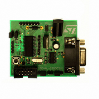
Manufacturer Part Number
STEVAL-ISQ002V1
Description
BOARD EVAL BASED ON ST72264G1
Manufacturer
STMicroelectronics
Specifications of STEVAL-ISQ002V1
Main Purpose
Interface, PMBus
Embedded
Yes, MCU, 8-Bit
Utilized Ic / Part
ST72F264
Primary Attributes
The PMBus™ Interface Using the ST7 I2C Peripheral
Secondary Attributes
Firmware in C Language
Product
Power Management Modules
Lead Free Status / RoHS Status
Lead free / RoHS Compliant
Other names
497-6423
Available stocks
Company
Part Number
Manufacturer
Quantity
Price
Company:

Part Number:
STEVAL-ISQ002V1
Manufacturer:
STMicroelectronics
Quantity:
1


ST72260Gx, ST72262Gx, ST72264Gx
6 SUPPLY, RESET AND CLOCK MANAGEMENT
The device includes a range of utility features for
securing the application in critical situations (for
example in case of a power brown-out), and re-
ducing the number of external components. An
overview is shown in
For more details, refer to dedicated parametric
section.
Main Features
■
■
■
■
Figure 10. Clock, Reset and Supply Block Diagram
20/172
RESET
OSC2
OSC1
V
V
– 4 Crystal/Ceramic resonator oscillators
– 1 Internal RC oscillator
– Main supply Low Voltage Detector (LVD)
– Auxiliary Voltage Detector (AVD) with inter-
Optional PLL for multiplying the frequency by 2
(not to be used with internal RC oscillator)
Reset Sequence Manager (RSM)
Multi-Oscillator Clock Management (MO)
System Integrity Management (SI)
SS
DD
rupt capability for monitoring the main supply
OSCILLATOR
RESET SEQUENCE
MULTI-
(MO)
MANAGER
(RSM)
Figure
f
OSC
10.
(option)
PLL
SYSTEM INTEGRITY MANAGEMENT
SICSR
0
AVD AVD LVD
IE
AVD Interrupt Request
AUXILIARY VOLTAGE
F
LOW VOLTAGE
6.1 PHASE LOCKED LOOP
If the clock frequency input to the PLL is in the 2 to
4 MHz range, the PLL can be used to multiply the
frequency by two to obtain an f
The PLL is enabled by option byte. If the PLL is
disabled, then f
Caution: The PLL is not recommended for appli-
cations where timing accuracy is required. See
“PLL Characteristics” on page 139.
Figure 9. PLL Block Diagram
RF
DETECTOR
DETECTOR
f
OSC
(AVD)
(LVD)
0
0
0
PLL x 2
WDG
f
OSC2 =
OSC2
/ 2
RF
CLOCK (MCC/RTC)
f
OSC
WITH REALTIME
MISCR1 Register
TIMER (WDG)
CONTROLLER
MAIN CLOCK
SLOW MODE
WATCHDOG
PLL OPTION BIT
SELECTION
/2.
OSC2
0
1
of 4 to 8 MHz.
f
f
OSC2
to CPU
and
Peripherals
CPU
Related parts for STEVAL-ISQ002V1
Image
Part Number
Description
Manufacturer
Datasheet
Request
R

Part Number:
Description:
BOARD RGB CTR ST7,STP08C596MTR
Manufacturer:
STMicroelectronics
Datasheet:

Part Number:
Description:
Power Management IC Development Tools Full Speed USB to RS232 Bridge Demo
Manufacturer:
STMicroelectronics
Datasheet:
Part Number:
Description:
Power Management IC Development Tools 2.5W solar eval BRD USB SPV1040 LD39050
Manufacturer:
STMicroelectronics
Datasheet:

Part Number:
Description:
BOARD EVAL FOR MEMS SENSORS
Manufacturer:
STMicroelectronics
Datasheet:

Part Number:
Description:
KIT DEV STARTER ST10F276Z5
Manufacturer:
STMicroelectronics
Datasheet:

Part Number:
Description:
BOARD EVAL HDMI $ VIDEO SWITCH
Manufacturer:
STMicroelectronics
Datasheet:

Part Number:
Description:
BOARD DEMO ACCELEROMETER DIL24
Manufacturer:
STMicroelectronics
Datasheet:

Part Number:
Description:
BOARD STLM75/STDS75/ST72F651
Manufacturer:
STMicroelectronics
Datasheet:

Part Number:
Description:
EVAL BOARD 3AXIS MEMS ACCELLRMTR
Manufacturer:
STMicroelectronics
Datasheet:

Part Number:
Description:
BOARD EVAL 8BIT MICRO + TDE1708
Manufacturer:
STMicroelectronics
Datasheet:
Part Number:
Description:
STMicroelectronics [RIPPLE-CARRY BINARY COUNTER/DIVIDERS]
Manufacturer:
STMicroelectronics
Datasheet:
Part Number:
Description:
STMicroelectronics [LIQUID-CRYSTAL DISPLAY DRIVERS]
Manufacturer:
STMicroelectronics
Datasheet:
Part Number:
Description:
BOARD EVAL FOR MEMS SENSORS
Manufacturer:
STMicroelectronics
Datasheet: