EVAL-ADUC831QSZ Analog Devices Inc, EVAL-ADUC831QSZ Datasheet - Page 11
EVAL-ADUC831QSZ
Manufacturer Part Number
EVAL-ADUC831QSZ
Description
KIT DEV FOR ADUC831 QUICK START
Manufacturer
Analog Devices Inc
Series
QuickStart™ Kitr
Type
MCUr
Datasheet
1.EVAL-ADUC831QSZ.pdf
(76 pages)
Specifications of EVAL-ADUC831QSZ
Contents
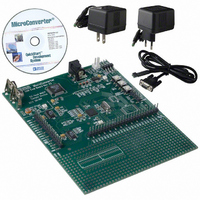
Evaluation Board, Power Supply, Cable, Software and Documentation
Silicon Manufacturer
Analog Devices
Core Architecture
8051
Silicon Core Number
ADuC831
Tool / Board Applications
General Purpose MCU, MPU, DSP, DSC
Mcu Supported Families
ADUC8xx
Development Tool Type
Hardware - Eval/Demo Board
Rohs Compliant
Yes
Lead Free Status / RoHS Status
Lead free / RoHS Compliant
For Use With/related Products
ADuC831
Lead Free Status / Rohs Status
Compliant
Other names
EVAL-ADUC831QS
EVAL-ADUC831QS
EVAL-ADUC831QS


The typical performance plots presented in this section illustrate
typical performance of the ADuC831 under various operating
conditions.
TPC 1 and TPC 2 below show typical ADC Integral Nonlinearity
(INL) errors from ADC code 0 to code 4095 at 5 V and 3 V
supplies respectively. The ADC is using its internal reference
(2.5 V) and operating at a sampling rate of 152 kHz and the
typically worst-case errors in both plots is just less than 0.3 LSBs.
TPC 3 and TPC 4 below show the variation in Worst Case
Positive (WCP) INL and Worst Case Negative (WCN) INL
versus external reference input voltage.
TPC 5 and TPC 6 show typical ADC differential nonlinearity
(DNL) errors from ADC code 0 to code 4095 at 5 V and 3 V sup-
plies, respectively. The ADC is using its internal reference (2. V) and
operating at a sampling rate of 152 kHz and the typically worst case
errors in both plots is just less than 0.2 LSBs.
TPC 7 and TPC 8 show the variation in worst case positive
(WCP) DNL and worst-case negative (WCN) DNL versus
external reference input voltage.
TPC 9 shows a histogram plot of 10,000 ADC conversion
results on a dc input with V
excellent code distribution pointing to the low noise perfor-
mance of the on-chip precision ADC.
REV. 0
–0.2
–0.4
–0.6
–0.8
–1.0
–0.2
–0.4
–0.6
–0.8
–1.0
0.8
0.4
1.0
0.8
0.6
0.4
0.2
1.0
0.6
0.2
0
0
0
0
TPC 1. Typical INL Error, V
TPC 2. Typical INL Error, V
511
511
1023
1023
1535
1535
DD
ADC CODES
ADC CODES
= 5 V. The plot illustrates an
2047
2047
2559
2559
AV
f
S
DD
DD
AV
f
3071
= 152kHz
3071
DD
S
= 5 V
= 3 V
= 152kHz
DD
/ DV
/DV
DD
3583
3583
DD
= 5V
Typical Performance Characteristics–ADuC831
= 3V
4095
4095
–11–
TPC 10 shows a histogram plot of 10,000 ADC conversion
results on a dc input for V
very tight code distribution of 1 LSB with the majority of codes
appearing in one output bin.
TPC 11 and TPC 12 show typical FFT plots for the ADuC831.
These plots were generated using an external clock input. The
ADC is using its internal reference (2.5 V) sampling a full-scale,
10 kHz sine wave test tone input at a sampling rate of 149.79 kHz.
The resultant FFTs shown at 5 V and 3 V supplies illustrate an
excellent 100 dB noise floor, 71 dB Signal-to-Noise Ratio (SNR)
and THD greater than –80 dB.
TPC 13 and TPC 14 show typical dynamic performance versus
external reference voltages. Again excellent ac performance can
be observed in both plots with some roll-off being observed as
V
TPC 15 shows typical dynamic performance versus sampling
frequency. SNR levels of 71 dBs are obtained across the sam-
pling range of the ADuC831.
TPC 16 shows the voltage output of the on-chip temperature
sensor versus temperature. Although the initial voltage output at
25ºC can vary from part to part, the resulting slope of
–2 mV/ºC is constant across all parts.
REF
TPC 4. Typical Worst Case INL Error vs. V
TPC 3. Typical Worst Case INL Error vs. V
falls below 1 V.
–0.2
–0.4
–0.6
–0.2
–0.4
–0.6
–0.8
1.2
1.0
0.8
0.6
0.4
0.2
0.8
0.6
0.4
0.2
0
0
0.5
0.5
1.0
1.0
EXTERNAL REFERENCE – V
EXTERNAL REFERENCE – V
DD
1.5
1.5
= 3 V. The plot again illustrates a
2.0
2.0
WCN INL
WCN INL
2.5
2.5
WCP INL
AV
WCP INL
f
AV
f
S
S
= 152kHz
DD
= 152kHz
DD
/DV
/DV
5.0
3.0
DD
REF,
DD
REF,
= 5V
= 3V
V
V
DD
DD
0.6
0.4
0.2
0
–0.2
–0.4
–0.6
0.8
0.6
0.4
0.2
–0.2
–0.4
–0.6
–0.8
0
= 3 V
= 5 V
Related parts for EVAL-ADUC831QSZ
Image
Part Number
Description
Manufacturer
Datasheet
Request
R


Part Number:
Description:
BOARD EVAL FOR SI270X-A
Manufacturer:
Silicon Laboratories Inc
Datasheet:

Part Number:
Description:
BUCK CONV REF DESIGN KIT IP1201
Manufacturer:
International Rectifier
Datasheet:
Part Number:
Description:
BOARD DEMO SYNC DUAL BUCK CNVTER
Manufacturer:
International Rectifier
Datasheet:
Part Number:
Description:
BOARD DEMO SYNC BUCK CONVETER
Manufacturer:
International Rectifier
Datasheet:

Part Number:
Description:
EVALBOARD/EB Omnidirectional microphone - Analog
Manufacturer:
Analog Devices
Datasheet:
Part Number:
Description:
EVALBOARD/EB Omnidirectional microphone - Analog
Manufacturer:
Analog Devices
Datasheet:


Part Number:
Description:
BOARD EVAL LED DRIVER LT3756
Manufacturer:
Linear Technology
Datasheet:

Part Number:
Description:
BOARD EVAL FOR AD7741/7742
Manufacturer:
Analog Devices Inc
Datasheet:

Part Number:
Description:
±1.7g Dual-Axis IMEMS Accelerometer Evaluation Board
Manufacturer:
Analog Devices Inc
Datasheet:

Part Number:
Description:
IC MULTIPLIER ANALOG 8-SOIC T/R
Manufacturer:
Analog Devices Inc
Datasheet:

Part Number:
Description:
IC ANALOG MULTIPLIER 8-DIP
Manufacturer:
Analog Devices Inc
Datasheet:
Part Number:
Description:
IC ANALOG MULTIPLIER 8-SOIC
Manufacturer:
Analog Devices Inc
Datasheet:
Part Number:
Description:
IC ANALOG MULTIPLIER 8-DIP
Manufacturer:
Analog Devices Inc
Datasheet: