EVAL-ADUC831QSZ Analog Devices Inc, EVAL-ADUC831QSZ Datasheet - Page 3
EVAL-ADUC831QSZ
Manufacturer Part Number
EVAL-ADUC831QSZ
Description
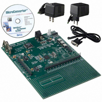
KIT DEV FOR ADUC831 QUICK START
Manufacturer
Analog Devices Inc
Series
QuickStart™ Kitr
Type
MCUr
Datasheet
1.EVAL-ADUC831QSZ.pdf
(76 pages)
Specifications of EVAL-ADUC831QSZ
Contents
Evaluation Board, Power Supply, Cable, Software and Documentation
Silicon Manufacturer
Analog Devices
Core Architecture
8051
Silicon Core Number
ADuC831
Tool / Board Applications
General Purpose MCU, MPU, DSP, DSC
Mcu Supported Families
ADUC8xx
Development Tool Type
Hardware - Eval/Demo Board
Rohs Compliant
Yes
Lead Free Status / RoHS Status
Lead free / RoHS Compliant
For Use With/related Products
ADuC831
Lead Free Status / Rohs Status
Compliant
Other names
EVAL-ADUC831QS
EVAL-ADUC831QS
EVAL-ADUC831QS


SPECIFICATIONS
Parameter
ADC CHANNEL SPECIFICATIONS
DC ACCURACY
CALIBRATED ENDPOINT ERRORS
DYNAMIC PERFORMANCE
ANALOG INPUT
TEMPERATURE SENSOR
DAC CHANNEL SPECIFICATIONS
DC ACCURACY
ANALOG OUTPUTS
DAC AC CHARACTERISTICS
REV. 0
Resolution
Integral Nonlinearity
Differential Nonlinearity
Integral Nonlinearity
Differential Nonlinearity
Code Distribution
Offset Error
Offset Error Match
Gain Error
Gain Error Match
Signal-to-Noise Ratio (SNR)
Total Harmonic Distortion (THD)
Peak Harmonic or Spurious Noise
Channel-to-Channel Crosstalk
Input Voltage Ranges
Leakage Current
Input Capacitance
Voltage Output at 25°C
Voltage TC
Accuracy
Internal Buffer Enabled
Resolution
Relative Accuracy
Differential Nonlinearity
Offset Error
Gain Error
Gain Error Mismatch
Voltage Range_0
Voltage Range_1
Output Impedance
Voltage Output Settling Time
Digital-to-Analog Glitch Energy
2, 3
10
4
4
11
9
7
8
1
(AV
all specifications T
DD
5, 6
= DV
V
12
± 1
± 0.3
± 0.9
± 0.25
± 1.5
+1.5/-0.9
1
± 4
± 1
± 2
–85
71
–85
–85
–80
0 to V
± 1
32
650
–2.0
± 3
± 1.5
12
± 3
–1
± 1/2
± 50
± 1
± 1
0.5
0 to V
0 to V
0.5
15
10
DD
DD
= 2.7 V to 3.3 V or 4.5 V to 5.5 V. V
= 5 V
REF
REF
DD
A
= T
MIN
to T
V
12
± 1
± 0.3
± 0.9
± 0.25
± 1.5
+1.5/–0.9
1
± 4
± 1
± 3
–85
71
–85
–85
–80
0 to V
± 1
32
650
–2.0
± 3
± 1.5
12
± 3
–1
± 1/2
± 50
± 1
± 1
0.5
0 to V
0 to V
0.5
15
10
DD
–3–
MAX
= 3 V
, unless otherwise noted.)
REF
REF
DD
Unit
LSB max
% typ
Bits
LSB max
LSB typ
LSB max
LSB typ
LSB max
LSB typ
LSB max
LSB typ
LSB max
dB typ
dB typ
dB typ
dB typ
dB typ
V
µA max
pF typ
mV typ
mV/°C typ
°C typ
°C typ
Bits
LSB typ
LSB max
LSB typ
mV max
% max
% typ
V typ
V typ
Ω typ
µs typ
nV sec typ
REF
= 2.5 V Internal Reference, MCLKIN = 16 MHz,
Test Conditions/Comments
f
Typical Performance at other f
2.5 V Internal Reference
2.5 V Internal Reference
1 V External Reference
1 V External Reference
ADC Input is a DC Voltage
f
f
Internal 2.5 V V
External 2.5 V V
DAC Load to AGND
R
Guaranteed 12-bit Monotonic
V
AV
V
% of Full Scale on DAC1
DAC V
DAC V
Full-Scale Settling Time to
within 1/2 LSB of Final Value
1 LSB Change at Major Carry
SAMPLE
IN
SAMPLE
L
REF
REF
= 10 kHz Sine Wave
= 10 kΩ, C
DD
Range
Range
Range
REF
REF
= 147 kHz, see Page 11 for
= 147 kHz
= 2.5 V
= V
L
DD
REF
= 100 pF
REF
ADuC831
SAMPLE
Related parts for EVAL-ADUC831QSZ
Image
Part Number
Description
Manufacturer
Datasheet
Request
R


Part Number:
Description:
BOARD EVAL FOR SI270X-A
Manufacturer:
Silicon Laboratories Inc
Datasheet:

Part Number:
Description:
BUCK CONV REF DESIGN KIT IP1201
Manufacturer:
International Rectifier
Datasheet:
Part Number:
Description:
BOARD DEMO SYNC DUAL BUCK CNVTER
Manufacturer:
International Rectifier
Datasheet:
Part Number:
Description:
BOARD DEMO SYNC BUCK CONVETER
Manufacturer:
International Rectifier
Datasheet:

Part Number:
Description:
EVALBOARD/EB Omnidirectional microphone - Analog
Manufacturer:
Analog Devices
Datasheet:
Part Number:
Description:
EVALBOARD/EB Omnidirectional microphone - Analog
Manufacturer:
Analog Devices
Datasheet:


Part Number:
Description:
BOARD EVAL LED DRIVER LT3756
Manufacturer:
Linear Technology
Datasheet:

Part Number:
Description:
BOARD EVAL FOR AD7741/7742
Manufacturer:
Analog Devices Inc
Datasheet:

Part Number:
Description:
±1.7g Dual-Axis IMEMS Accelerometer Evaluation Board
Manufacturer:
Analog Devices Inc
Datasheet:

Part Number:
Description:
IC MULTIPLIER ANALOG 8-SOIC T/R
Manufacturer:
Analog Devices Inc
Datasheet:

Part Number:
Description:
IC ANALOG MULTIPLIER 8-DIP
Manufacturer:
Analog Devices Inc
Datasheet:
Part Number:
Description:
IC ANALOG MULTIPLIER 8-SOIC
Manufacturer:
Analog Devices Inc
Datasheet:
Part Number:
Description:
IC ANALOG MULTIPLIER 8-DIP
Manufacturer:
Analog Devices Inc
Datasheet: