EVAL-ADUC831QSZ Analog Devices Inc, EVAL-ADUC831QSZ Datasheet - Page 9
EVAL-ADUC831QSZ
Manufacturer Part Number
EVAL-ADUC831QSZ
Description
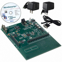
KIT DEV FOR ADUC831 QUICK START
Manufacturer
Analog Devices Inc
Series
QuickStart™ Kitr
Type
MCUr
Datasheet
1.EVAL-ADUC831QSZ.pdf
(76 pages)
Specifications of EVAL-ADUC831QSZ
Contents
Evaluation Board, Power Supply, Cable, Software and Documentation
Silicon Manufacturer
Analog Devices
Core Architecture
8051
Silicon Core Number
ADuC831
Tool / Board Applications
General Purpose MCU, MPU, DSP, DSC
Mcu Supported Families
ADUC8xx
Development Tool Type
Hardware - Eval/Demo Board
Rohs Compliant
Yes
Lead Free Status / RoHS Status
Lead free / RoHS Compliant
For Use With/related Products
ADuC831
Lead Free Status / Rohs Status
Compliant
Other names
EVAL-ADUC831QS
EVAL-ADUC831QS
EVAL-ADUC831QS


Mnemonic
DV
AV
C
V
AGND
P1.0–P1.7
ADC0–ADC7 I
T2
T2EX
SS
SDATA
SCLOCK
MOSI
MISO
DAC0
DAC1
RESET
P3.0–P3.7
PWMC
PWM0
PWM1
RxD
TxD
INT0
INT1
T0
T1
CONVST
WR
RD
XTAL2
XTAL1
DGND
P2.0–P2.7
(A8–A15)
(A16–A23)
REV. 0
REF
REF
DD
DD
I
I/O
I/O
Type Function
P
P
I
I/O
G
I
I
I
I/O
I/O
I/O
I/O
O
O
I
I
O
O
I/O
O
I
I
I
I
I
O
O
O
I
G
Digital Positive Supply Voltage, 3 V or 5 V Nominal
Analog Positive Supply Voltage, 3 V or 5 V Nominal
Decoupling Input for On-Chip Reference. Connect 0.1 µF between this pin and AGND.
Reference Input/Output. This pin is connected to the internal reference through a series resistor and is the
reference source for the analog-to-digital converter. The nominal internal reference voltage is 2.5 V and this
appears at the pin. This pin can be overdriven by an external reference.
Analog Ground. Ground reference point for the analog circuitry.
Port 1 is an 8-bit input port only. Unlike other ports, Port 1 defaults to Analog Input mode, to configure
any of these Port Pins as a digital input, write a “0” to the port bit. Port 1 pins are multifunction and share
the following functionality.
Analog Inputs. Eight single-ended analog inputs. Channel selection is via ADCCON2 SFR.
Timer 2 Digital Input. Input to Timer/Counter 2. When enabled, Counter 2 is incremented in response to a
1-to-0 transition of the T2 input.
Digital Input. Capture/Reload trigger for Counter 2 and also functions as an Up/Down control input for
Counter 2.
Slave Select Input for the SPI Interface
User Selectable, I
Serial Clock Pin for I
SPI Master Output/Slave Input Data I/O Pin for SPI Interface
SPI Master Input/Slave Output Data I/O Pin for SPI Serial Interface
Voltage Output from DAC0
Voltage Output from DAC1
Digital Input. A high level on this pin for 24 master clock cycles while the oscillator is running resets the device.
Port 3 is a bidirectional port with internal pull-up resistors. Port 3 pins that have 1s written to them are
pulled high by the internal pull-up resistors, and in that state they can be used as inputs. As inputs, Port 3
pins being pulled externally low will source current because of the internal pull-up resistors. Port 3 pins
also contain various secondary functions which are described below.
PWM Clock Input
PWM0 Voltage Output. PWM outputs can be configured to use ports 2.6 and 2.7, or 3.4 and 3.3.
PWM1 Voltage Output. See CFG831 Register for further information.
Receiver Data Input (Asynchronous) or Data Input/Output (Synchronous) of Serial (UART) Port
Transmitter Data Output (Asynchronous) or Clock Output (Synchronous) of Serial (UART) Port
Interrupt 0, programmable edge- or level-triggered Interrupt input, which can be programmed to one of two
priority levels. This pin can also be used as a gate control input to Timer 0.
Interrupt 1, programmable edge- or level-triggered Interrupt input, which can be programmed to one of two
priority levels. This pin can also be used as a gate control input to Timer 1.
Timer/Counter 0 Input
Timer/Counter 1 Input
Active Low Convert Start Logic Input for the ADC Block when the External Convert Start Function is Enabled.
A low-to-high transition on this input puts the track-and-hold into its hold mode and starts conversion.
Write Control Signal, Logic Output. Latches the data byte from Port 0 into the external data memory.
Read Control Signal, Logic Output. Enables the external data memory to Port 0.
Output of the Inverting Oscillator Amplifier
Input to the Inverting Oscillator Amplifier, and input to the internal clock generator circuits.
Digital Ground. Ground reference point for the digital circuitry.
Port 2 is a bidirectional port with internal pull-up resistors. Port 2 pins that have 1s written to them are
pulled high by the internal pull-up resistors, and in that state they can be used as inputs. As inputs, Port 2
pins being pulled externally low will source current because of the internal pull-up resistors. Port 2 emits
the high order address bytes during fetches from external program memory and middle and high order
address bytes during accesses to the external 24-bit external data memory space.
2
C Compatible or SPI Data Input/Output Pin
2
C Compatible or SPI Serial Interface Clock
PIN FUNCTION DESCRIPTIONS
–9–
ADuC831
Related parts for EVAL-ADUC831QSZ
Image
Part Number
Description
Manufacturer
Datasheet
Request
R


Part Number:
Description:
BOARD EVAL FOR SI270X-A
Manufacturer:
Silicon Laboratories Inc
Datasheet:

Part Number:
Description:
BUCK CONV REF DESIGN KIT IP1201
Manufacturer:
International Rectifier
Datasheet:
Part Number:
Description:
BOARD DEMO SYNC DUAL BUCK CNVTER
Manufacturer:
International Rectifier
Datasheet:
Part Number:
Description:
BOARD DEMO SYNC BUCK CONVETER
Manufacturer:
International Rectifier
Datasheet:

Part Number:
Description:
EVALBOARD/EB Omnidirectional microphone - Analog
Manufacturer:
Analog Devices
Datasheet:
Part Number:
Description:
EVALBOARD/EB Omnidirectional microphone - Analog
Manufacturer:
Analog Devices
Datasheet:


Part Number:
Description:
BOARD EVAL LED DRIVER LT3756
Manufacturer:
Linear Technology
Datasheet:

Part Number:
Description:
BOARD EVAL FOR AD7741/7742
Manufacturer:
Analog Devices Inc
Datasheet:

Part Number:
Description:
±1.7g Dual-Axis IMEMS Accelerometer Evaluation Board
Manufacturer:
Analog Devices Inc
Datasheet:

Part Number:
Description:
IC MULTIPLIER ANALOG 8-SOIC T/R
Manufacturer:
Analog Devices Inc
Datasheet:

Part Number:
Description:
IC ANALOG MULTIPLIER 8-DIP
Manufacturer:
Analog Devices Inc
Datasheet:
Part Number:
Description:
IC ANALOG MULTIPLIER 8-SOIC
Manufacturer:
Analog Devices Inc
Datasheet:
Part Number:
Description:
IC ANALOG MULTIPLIER 8-DIP
Manufacturer:
Analog Devices Inc
Datasheet: