EVAL-ADUC831QSZ Analog Devices Inc, EVAL-ADUC831QSZ Datasheet - Page 60
EVAL-ADUC831QSZ
Manufacturer Part Number
EVAL-ADUC831QSZ
Description
KIT DEV FOR ADUC831 QUICK START
Manufacturer
Analog Devices Inc
Series
QuickStart™ Kitr
Type
MCUr
Datasheet
1.EVAL-ADUC831QSZ.pdf
(76 pages)
Specifications of EVAL-ADUC831QSZ
Contents
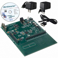
Evaluation Board, Power Supply, Cable, Software and Documentation
Silicon Manufacturer
Analog Devices
Core Architecture
8051
Silicon Core Number
ADuC831
Tool / Board Applications
General Purpose MCU, MPU, DSP, DSC
Mcu Supported Families
ADUC8xx
Development Tool Type
Hardware - Eval/Demo Board
Rohs Compliant
Yes
Lead Free Status / RoHS Status
Lead free / RoHS Compliant
For Use With/related Products
ADuC831
Lead Free Status / Rohs Status
Compliant
Other names
EVAL-ADUC831QS
EVAL-ADUC831QS
EVAL-ADUC831QS


ADuC831
Interrupt Priority
The Interrupt Enable registers are written by the user to enable
individual interrupt sources, while the Interrupt Priority registers
allow the user to select one of two priority levels for each interrupt.
An interrupt of a high priority may interrupt the service routine
of a low priority interrupt, and if two interrupts of different
priority occur at the same time, the higher level interrupt will be
serviced first. An interrupt cannot be interrupted by another
interrupt of the same priority level. If two interrupts of the same
priority level occur simultaneously, a polling sequence is observed
as shown in Table XXXI.
Source
PSMI
WDS
IE0
ADCI
TF0
IE1
TF1
I2CI + ISPI
RI + TI
TF2 + EXF2 9 (Lowest)
TII
Interrupt Vectors
When an interrupt occurs, the program counter is pushed onto
the stack and the corresponding interrupt vector address is
loaded into the program counter. The Interrupt Vector Addresses
are shown in Table XXXII.
Table XXXI. Priority within an Interrupt Level
Source
IE0
TF0
IE1
TF1
RI + TI
TF2 + EXF2
ADCI
I2CI + ISPI
PSMI
TII
WDS
Table XXXII. Interrupt Vector Addresses
Priority
1 (Highest)
2
2
3
4
5
6
7
8
11 (Lowest)
Description
Power Supply Monitor Interrupt
Watchdog Timer Interrupt
External Interrupt 0
ADC Interrupt
Timer/Counter 0 Interrupt
External Interrupt 1
Timer/Counter 1 Interrupt
SPI Interrupt
Serial Interrupt
Timer/Counter 2 Interrupt
Time Interval Counter Interrupt
0003H
000BH
0013H
001BH
0023H
002BH
0033H
003BH
0043H
0053H
005BH
Vector Address
–60–
ADuC831 HARDWARE DESIGN CONSIDERATIONS
This section outlines some of the key hardware design consider-
ations that must be addressed when integrating the ADuC831
into any hardware system.
Clock Oscillator
The clock source for the ADuC831 can come either from an
external source or from the internal clock oscillator. To use the
internal clock oscillator, connect a parallel resonant crystal between
XTAL1 and XTAL2, and connect a capacitor from each pin to
ground as shown below.
Whether using the internal oscillator or an external clock
source, the ADuC831’s specified operational clock speed range is
400 kHz to 16 MHz. The core itself is static, and will function
all the way down to dc. But at clock speeds slower that 400 kHz
the ADC will no longer function correctly. Therefore, to ensure
specified operation, use a clock frequency of at least 400 kHz
and no more than 16 MHz. Note: the Flash/EE memory may
not program correctly at a clock frequency of less than 2 MHz.
External Memory Interface
In addition to its internal program and data memories, the ADuC831
can access up to 64 kBytes of external program memory (ROM/
PROM/etc.) and up to 16 MBytes of external data memory (SRAM).
To select from which code space (internal or external program
memory) to begin executing instructions, tie the EA (external
access) pin high or low, respectively. When EA is high (pulled up
to V
internal 62 kBytes Flash/EE code space. When EA is low (tied
to ground) user program execution will start at address 0 of the
external code space.
A second very important function of the EA pin is described
in the Single Pin Emulation Mode section.
External program memory (if used) must be connected to the
ADuC831 as illustrated in Figure 57. Note that 16 I/O lines
Figure 55. External Parallel Resonant Crystal Connections
DD
Figure 56. Connecting an External Clock Source
), user program execution will start at address 0 of the
EXTERNAL
SOURCE
CLOCK
XTAL1
XTAL2
XTAL1
XTAL2
ADuC831
ADuC831
TO INTERNAL
TIMNG CIRCUITS
TO INTERNAL
TIMNG CIRCUITS
REV. 0
Related parts for EVAL-ADUC831QSZ
Image
Part Number
Description
Manufacturer
Datasheet
Request
R


Part Number:
Description:
BOARD EVAL FOR SI270X-A
Manufacturer:
Silicon Laboratories Inc
Datasheet:

Part Number:
Description:
BUCK CONV REF DESIGN KIT IP1201
Manufacturer:
International Rectifier
Datasheet:
Part Number:
Description:
BOARD DEMO SYNC DUAL BUCK CNVTER
Manufacturer:
International Rectifier
Datasheet:
Part Number:
Description:
BOARD DEMO SYNC BUCK CONVETER
Manufacturer:
International Rectifier
Datasheet:

Part Number:
Description:
EVALBOARD/EB Omnidirectional microphone - Analog
Manufacturer:
Analog Devices
Datasheet:
Part Number:
Description:
EVALBOARD/EB Omnidirectional microphone - Analog
Manufacturer:
Analog Devices
Datasheet:


Part Number:
Description:
BOARD EVAL LED DRIVER LT3756
Manufacturer:
Linear Technology
Datasheet:

Part Number:
Description:
BOARD EVAL FOR AD7741/7742
Manufacturer:
Analog Devices Inc
Datasheet:

Part Number:
Description:
±1.7g Dual-Axis IMEMS Accelerometer Evaluation Board
Manufacturer:
Analog Devices Inc
Datasheet:

Part Number:
Description:
IC MULTIPLIER ANALOG 8-SOIC T/R
Manufacturer:
Analog Devices Inc
Datasheet:

Part Number:
Description:
IC ANALOG MULTIPLIER 8-DIP
Manufacturer:
Analog Devices Inc
Datasheet:
Part Number:
Description:
IC ANALOG MULTIPLIER 8-SOIC
Manufacturer:
Analog Devices Inc
Datasheet:
Part Number:
Description:
IC ANALOG MULTIPLIER 8-DIP
Manufacturer:
Analog Devices Inc
Datasheet: