EVAL-ADUC831QSZ Analog Devices Inc, EVAL-ADUC831QSZ Datasheet - Page 31
EVAL-ADUC831QSZ
Manufacturer Part Number
EVAL-ADUC831QSZ
Description
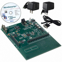
KIT DEV FOR ADUC831 QUICK START
Manufacturer
Analog Devices Inc
Series
QuickStart™ Kitr
Type
MCUr
Datasheet
1.EVAL-ADUC831QSZ.pdf
(76 pages)
Specifications of EVAL-ADUC831QSZ
Contents
Evaluation Board, Power Supply, Cable, Software and Documentation
Silicon Manufacturer
Analog Devices
Core Architecture
8051
Silicon Core Number
ADuC831
Tool / Board Applications
General Purpose MCU, MPU, DSP, DSC
Mcu Supported Families
ADUC8xx
Development Tool Type
Hardware - Eval/Demo Board
Rohs Compliant
Yes
Lead Free Status / RoHS Status
Lead free / RoHS Compliant
For Use With/related Products
ADuC831
Lead Free Status / Rohs Status
Compliant
Other names
EVAL-ADUC831QS
EVAL-ADUC831QS
EVAL-ADUC831QS


ADuC831 Configuration SFR (CFG831)
The CFG831 SFR contains the necessary bits to configure the
internal XRAM, EPROM controller, PWM output selection
and frequency, DAC buffer, and the extended SP. By default it
configures the user into 8051 mode, i.e., extended SP is disabled,
internal XRAM is disabled.
CFG831
SFR Address
Power-On Default Value
Bit Addressable
*Note that the Flash/EE controller bits EPM2, EPM1, EPM0 are set to their
REV. 0
Bit
7
6
5
4
3
2
1
0
correct values depending on the crystal frequency at power-up. The user should
not modify these bits so all instructions to the CFG831 register should use the
ORL, XRL, or ANL instructions. Value of 10H is for a 11.0592 MHz crystal.
Name
EXSP
PWPO
DBUF
EPM2
EPM1
EPM0
RSVD
XRAMEN
Description
Extended SP Enable.
When set to “1” by the user, the stack will rollover from SPH/SP = 00FFH to 0100H.
When set to “0” by the user, the stack will roll over from SP = FFH to SP = 00H.
PWM Pin Out Selection.
Set to “1” by the user = PWM output pins selected as P3.4 and P3.3.
Set to “0” by the user = PWM output pins selected as P2.6 and P2.7.
DAC Output Buffer.
Set to “1” by the user = DAC
Set to “0” by the user = DAC Output Buffer Enabled.
Flash/EE Controller and PWM Clock Frequency Configuration Bits.
Frequency should be configured such that Fosc/Divide Factor = 32 kHz + 50%.
EPM2 EPM1 EPM0
0
0
0
0
1
1
Reserved. This bit should always contain 0.
XRAM Enable Bit.
When set to “1” the internal XRAM will be mapped into the lower 2 kBytes of the external address space.
When set to “0” the internal XRAM will not be accessible and the external data memory will be mapped
into the lower 2 kBytes of external data memory.
ADuC831 Config SFR
AFH
10*H
No
0
0
1
1
0
0
0
1
0
1
0
1
Table VIII. CFG831 SFR Bit Designations
.
Output Buffer Bypassed.
Divide Factor
32
64
128
256
512
1024
–31–
ADuC831
Related parts for EVAL-ADUC831QSZ
Image
Part Number
Description
Manufacturer
Datasheet
Request
R


Part Number:
Description:
BOARD EVAL FOR SI270X-A
Manufacturer:
Silicon Laboratories Inc
Datasheet:

Part Number:
Description:
BUCK CONV REF DESIGN KIT IP1201
Manufacturer:
International Rectifier
Datasheet:
Part Number:
Description:
BOARD DEMO SYNC DUAL BUCK CNVTER
Manufacturer:
International Rectifier
Datasheet:
Part Number:
Description:
BOARD DEMO SYNC BUCK CONVETER
Manufacturer:
International Rectifier
Datasheet:

Part Number:
Description:
EVALBOARD/EB Omnidirectional microphone - Analog
Manufacturer:
Analog Devices
Datasheet:
Part Number:
Description:
EVALBOARD/EB Omnidirectional microphone - Analog
Manufacturer:
Analog Devices
Datasheet:


Part Number:
Description:
BOARD EVAL LED DRIVER LT3756
Manufacturer:
Linear Technology
Datasheet:

Part Number:
Description:
BOARD EVAL FOR AD7741/7742
Manufacturer:
Analog Devices Inc
Datasheet:

Part Number:
Description:
±1.7g Dual-Axis IMEMS Accelerometer Evaluation Board
Manufacturer:
Analog Devices Inc
Datasheet:

Part Number:
Description:
IC MULTIPLIER ANALOG 8-SOIC T/R
Manufacturer:
Analog Devices Inc
Datasheet:

Part Number:
Description:
IC ANALOG MULTIPLIER 8-DIP
Manufacturer:
Analog Devices Inc
Datasheet:
Part Number:
Description:
IC ANALOG MULTIPLIER 8-SOIC
Manufacturer:
Analog Devices Inc
Datasheet:
Part Number:
Description:
IC ANALOG MULTIPLIER 8-DIP
Manufacturer:
Analog Devices Inc
Datasheet: