DEMO9S08LC60 Freescale Semiconductor, DEMO9S08LC60 Datasheet - Page 231
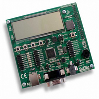
DEMO9S08LC60
Manufacturer Part Number
DEMO9S08LC60
Description
BOARD DEMO FOR 9S08LC60
Manufacturer
Freescale Semiconductor
Type
MCUr
Datasheets
1.DEMO9S08LC60.pdf
(360 pages)
2.DEMO9S08LC60.pdf
(32 pages)
3.DEMO9S08LC60.pdf
(2 pages)
Specifications of DEMO9S08LC60
Contents
Evaluation Board
Processor To Be Evaluated
MC9S08LC60
Interface Type
RS-232, USB
Silicon Manufacturer
Freescale
Core Architecture
HCS08
Core Sub-architecture
HCS08
Silicon Core Number
MC9S08
Silicon Family Name
S08LC
Rohs Compliant
Yes
For Use With/related Products
MC9S08LC60
Lead Free Status / RoHS Status
Lead free / RoHS Compliant


If the bit value to be transmitted as the ninth bit of a new character is the same as for the previous character,
it is not necessary to write to T8 again. When data is transferred from the transmit data buffer to the
transmit shifter, the value in T8 is copied at the same time data is transferred from SCID to the shifter.
9-bit data mode typically is used in conjunction with parity to allow eight bits of data plus the parity in the
ninth bit. Or it is used with address-mark wakeup so the ninth data bit can serve as the wakeup bit. In
custom protocols, the ninth bit can also serve as a software-controlled marker.
12.4.2
During all stop modes, clocks to the SCI module are halted.
In stop1 and stop2 modes, all SCI register data is lost and must be re-initialized upon recovery from these
two stop modes.
No SCI module registers are affected in stop3 mode.
Note, because the clocks are halted, the SCI module will resume operation upon exit from stop (only in
stop3 mode). Software should ensure stop mode is not entered while there is a character being transmitted
out of or received into the SCI module.
12.4.3
When LOOPS = 1, the RSRC bit in the same register chooses between loop mode (RSRC = 0) or
single-wire mode (RSRC = 1). Loop mode is sometimes used to check software, independent of
connections in the external system, to help isolate system problems. In this mode, the transmitter output is
internally connected to the receiver input and the RxD1 pin is not used by the SCI, so it reverts to a
general-purpose port I/O pin.
12.4.4
When LOOPS = 1, the RSRC bit in the same register chooses between loop mode (RSRC = 0) or
single-wire mode (RSRC = 1). Single-wire mode is used to implement a half-duplex serial connection.
The receiver is internally connected to the transmitter output and to the TxD1 pin. The RxD1 pin is not
used and reverts to a general-purpose port I/O pin.
In single-wire mode, the TXDIR bit in SCIC3 controls the direction of serial data on the TxD1 pin. When
TXDIR = 0, the TxD1 pin is an input to the SCI receiver and the transmitter is temporarily disconnected
from the TxD1 pin so an external device can send serial data to the receiver. When TXDIR = 1, the TxD1
pin is an output driven by the transmitter. In single-wire mode, the internal loop back connection from the
transmitter to the receiver causes the receiver to receive characters that are sent out by the transmitter.
Freescale Semiconductor
Stop Mode Operation
Loop Mode
Single-Wire Operation
MC9S08LC60 Series Data Sheet: Technical Data, Rev. 4
Chapter 12 Serial Communications Interface (S08SCIV3)
231
Related parts for DEMO9S08LC60
Image
Part Number
Description
Manufacturer
Datasheet
Request
R

Part Number:
Description:
Manufacturer:
Freescale Semiconductor, Inc
Datasheet:
Part Number:
Description:
Manufacturer:
Freescale Semiconductor, Inc
Datasheet:
Part Number:
Description:
Manufacturer:
Freescale Semiconductor, Inc
Datasheet:
Part Number:
Description:
Manufacturer:
Freescale Semiconductor, Inc
Datasheet:
Part Number:
Description:
Manufacturer:
Freescale Semiconductor, Inc
Datasheet:
Part Number:
Description:
Manufacturer:
Freescale Semiconductor, Inc
Datasheet:
Part Number:
Description:
Manufacturer:
Freescale Semiconductor, Inc
Datasheet:
Part Number:
Description:
Manufacturer:
Freescale Semiconductor, Inc
Datasheet:
Part Number:
Description:
Manufacturer:
Freescale Semiconductor, Inc
Datasheet:
Part Number:
Description:
Manufacturer:
Freescale Semiconductor, Inc
Datasheet:
Part Number:
Description:
Manufacturer:
Freescale Semiconductor, Inc
Datasheet:
Part Number:
Description:
Manufacturer:
Freescale Semiconductor, Inc
Datasheet:
Part Number:
Description:
Manufacturer:
Freescale Semiconductor, Inc
Datasheet:
Part Number:
Description:
Manufacturer:
Freescale Semiconductor, Inc
Datasheet:
Part Number:
Description:
Manufacturer:
Freescale Semiconductor, Inc
Datasheet: