DEMO9S08LC60 Freescale Semiconductor, DEMO9S08LC60 Datasheet - Page 30
DEMO9S08LC60
Manufacturer Part Number
DEMO9S08LC60
Description
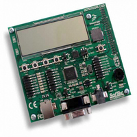
BOARD DEMO FOR 9S08LC60
Manufacturer
Freescale Semiconductor
Type
MCUr
Datasheets
1.DEMO9S08LC60.pdf
(360 pages)
2.DEMO9S08LC60.pdf
(32 pages)
3.DEMO9S08LC60.pdf
(2 pages)
Specifications of DEMO9S08LC60
Contents
Evaluation Board
Processor To Be Evaluated
MC9S08LC60
Interface Type
RS-232, USB
Silicon Manufacturer
Freescale
Core Architecture
HCS08
Core Sub-architecture
HCS08
Silicon Core Number
MC9S08
Silicon Family Name
S08LC
Rohs Compliant
Yes
For Use With/related Products
MC9S08LC60
Lead Free Status / RoHS Status
Lead free / RoHS Compliant


Chapter 2 Pins and Connections
2.3.4
After POR, the configuration of the PTB2/RESET pin defaults to RESET. Clearing the RSTPE bit in
SOPT1 register configures the pin to be the PTB2 general-purpose, output only pin. After configured as
PTB2, the pin will remain PTB2 until the next reset. The RESET pin can be used to reset the MCU from
an external source when the pin is driven low.
When enabled as the RESET pin (RSTPE = 1), an internal pullup device is automatically enabled. It has
input hysteresis, a high current output driver, and no output slew rate control. Internal power-on reset and
low-voltage reset circuitry typically make external reset circuitry unnecessary.
The PTB2/RESET pin will default to the RESET pin when a POR enters active background mode. This
pin is normally connected to the standard 6-pin background debug connector so a development system can
directly reset the MCU system. If desired, when the pin is configured as the RESET pin, a manual external
reset can be added by supplying a simple switch to ground (pull reset pin low to force a reset).
Whenever any reset is initiated (whether from an external signal or from an internal system), the reset pin
is driven low for approximately 34 cycles of f
cycles of f
timeout, the circuitry expects the reset pin sample to return a logic 1. The reset circuitry decodes the cause
of reset and records it by setting a corresponding bit in the system control reset status register (SRS).
In EMC-sensitive applications, an external RC filter is recommended on the reset pin. See
an example.
2.3.5
The background / mode select (BKGD/MS) shares its function with an output-only port pin, PTC6. While
in reset, the pin functions as a mode select pin. Immediately after reset rises the pin functions as the
background pin and can be used for background debug communication. While functioning as a
background/mode select pin (BKGDPE = 1), the pin includes an internal pullup device, input hysteresis,
a standard output driver, and no output slew rate control. When used as an I/O port, the pin is limited to
output only.
If nothing is connected to this pin, the MCU will enter normal operating mode at the rising edge of reset.
If a debug system is connected to the 6-pin standard background debug header, it can hold BKGD/MS low
during the rising edge of reset which forces the MCU to active background mode.
The BKGD pin is used primarily for background debug controller (BDC) communications using a custom
protocol that uses 16 clock cycles of the target MCU’s BDC clock per bit time. The target MCU’s BDC
clock could be as fast as the bus clock rate, so there should never be any significant capacitance connected
to the BKGD/MS pin that could interfere with background serial communications.
Although the BKGD pin is a pseudo open-drain pin, the background debug communication protocol
provides brief, actively driven, high speedup pulses to ensure fast rise times. Small capacitances from
cables and the absolute value of the internal pullup device play almost no role in determining rise and fall
times on the BKGD pin.
30
Self_reset
RESET Pin
Background / Mode Select (BKGD/MS)
later. If reset was caused by an internal source such as low-voltage reset or watchdog
MC9S08LC60 Series Data Sheet: Technical Data, Rev. 4
Self_reset
, released, and sampled again approximately 38
Freescale Semiconductor
Figure 2-3
for
Related parts for DEMO9S08LC60
Image
Part Number
Description
Manufacturer
Datasheet
Request
R

Part Number:
Description:
Manufacturer:
Freescale Semiconductor, Inc
Datasheet:
Part Number:
Description:
Manufacturer:
Freescale Semiconductor, Inc
Datasheet:
Part Number:
Description:
Manufacturer:
Freescale Semiconductor, Inc
Datasheet:
Part Number:
Description:
Manufacturer:
Freescale Semiconductor, Inc
Datasheet:
Part Number:
Description:
Manufacturer:
Freescale Semiconductor, Inc
Datasheet:
Part Number:
Description:
Manufacturer:
Freescale Semiconductor, Inc
Datasheet:
Part Number:
Description:
Manufacturer:
Freescale Semiconductor, Inc
Datasheet:
Part Number:
Description:
Manufacturer:
Freescale Semiconductor, Inc
Datasheet:
Part Number:
Description:
Manufacturer:
Freescale Semiconductor, Inc
Datasheet:
Part Number:
Description:
Manufacturer:
Freescale Semiconductor, Inc
Datasheet:
Part Number:
Description:
Manufacturer:
Freescale Semiconductor, Inc
Datasheet:
Part Number:
Description:
Manufacturer:
Freescale Semiconductor, Inc
Datasheet:
Part Number:
Description:
Manufacturer:
Freescale Semiconductor, Inc
Datasheet:
Part Number:
Description:
Manufacturer:
Freescale Semiconductor, Inc
Datasheet:
Part Number:
Description:
Manufacturer:
Freescale Semiconductor, Inc
Datasheet: