M68EVB908GB60E Freescale Semiconductor, M68EVB908GB60E Datasheet - Page 192
M68EVB908GB60E
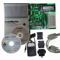
Manufacturer Part Number
M68EVB908GB60E
Description
BOARD EVAL FOR MC9S08GB60
Manufacturer
Freescale Semiconductor
Type
MCUr
Datasheet
1.M68EVB908GB60E.pdf
(290 pages)
Specifications of M68EVB908GB60E
Contents
Module and Misc Hardware
Processor To Be Evaluated
MC9S08GB
Data Bus Width
8 bit
Interface Type
RS-232
Silicon Manufacturer
Freescale
Core Architecture
HCS08
Core Sub-architecture
HCS08
Silicon Core Number
MC9S08
Silicon Family Name
S08GB
Kit Contents
GB60 Evaluation Kit
Rohs Compliant
Yes
For Use With/related Products
MC9S08GB60
Lead Free Status / RoHS Status
Lead free / RoHS Compliant


Serial Peripheral Interface (SPI) Module
12.2.3
As shown in
prescale bits (SPPR2:SPPR1:SPPR0) choose a prescale divisor of 1, 2, 3, 4, 5, 6, 7, or 8. The three rate
select bits (SPR2:SPR1:SPR0) divide the output of the prescaler stage by 2, 4, 8, 16, 32, 64, 128, or 256
to get the internal SPI master mode bit-rate clock.
12.3
An SPI transfer is initiated by checking for the SPI transmit buffer empty flag (SPTEF = 1) and then
writing a byte of data to the SPI data register (SPI1D) in the master SPI device. When the SPI shift register
is available, this byte of data is moved from the transmit data buffer to the shifter, SPTEF is set to indicate
there is room in the buffer to queue another transmit character if desired, and the SPI serial transfer starts.
During the SPI transfer, data is sampled (read) on the MISO1 pin at one SPSCK edge and shifted, changing
the bit value on the MOSI1 pin, one-half SPSCK cycle later. After eight SPSCK cycles, the data that was
in the shift register of the master has been shifted out the MOSI1 pin to the slave while eight bits of data
were shifted in the MISO1 pin into the master’s shift register. At the end of this transfer, the received data
byte is moved from the shifter into the receive data buffer and SPRF is set to indicate the data can be read
by reading SPI1D. If another byte of data is waiting in the transmit buffer at the end of a transfer, it is
moved into the shifter, SPTEF is set, and a new transfer is started.
Normally, SPI data is transferred most significant bit (MSB) first. If the least significant bit first enable
(LSBFE) bit is set, SPI data is shifted LSB first.
When the SPI is configured as a slave, its SS1 pin must be driven low before a transfer starts and SS1 must
stay low throughout the transfer. If a clock format where CPHA = 0 is selected, SS1 must be driven to a
logic 1 between successive transfers. If CPHA = 1, SS1 may remain low between successive transfers. See
Section 12.3.1, “SPI Clock
Because the transmitter and receiver are double buffered, a second byte, in addition to the byte currently
being shifted out, can be queued into the transmit data buffer, and a previously received character can be
in the receive data buffer while a new character is being shifted in. The SPTEF flag indicates when the
transmit buffer has room for a new character. The SPRF flag indicates when a received character is
available in the receive data buffer. The received character must be read out of the receive buffer (read
SPI1D) before the next transfer is finished or a receive overrun error results.
In the case of a receive overrun, the new data is lost because the receive buffer still held the previous
character and was not ready to accept the new data. There is no indication for such an overrun condition
so the application system designer must ensure that previous data has been read from the receive buffer
before a new transfer is initiated.
192
Functional Description
SPI Baud Rate Generation
Figure
BUS CLOCK
12-4, the clock source for the SPI baud rate generator is the bus clock. The three
Formats,”
SPPR2:SPPR1:SPPR0
1, 2, 3, 4, 5, 6, 7, or 8
Figure 12-4. SPI Baud Rate Generation
PRESCALER
DIVIDE BY
MC9S08GB/GT Data Sheet, Rev. 2.3
for more details.
2, 4, 8, 16, 32, 64, 128, or 256
CLOCK RATE DIVIDER
SPR2:SPR1:SPR0
DIVIDE BY
MASTER
SPI
BIT RATE
Freescale Semiconductor
Related parts for M68EVB908GB60E
Image
Part Number
Description
Manufacturer
Datasheet
Request
R

Part Number:
Description:
Manufacturer:
Freescale Semiconductor, Inc
Datasheet:
Part Number:
Description:
Manufacturer:
Freescale Semiconductor, Inc
Datasheet:
Part Number:
Description:
Manufacturer:
Freescale Semiconductor, Inc
Datasheet:
Part Number:
Description:
Manufacturer:
Freescale Semiconductor, Inc
Datasheet:
Part Number:
Description:
Manufacturer:
Freescale Semiconductor, Inc
Datasheet:
Part Number:
Description:
Manufacturer:
Freescale Semiconductor, Inc
Datasheet:
Part Number:
Description:
Manufacturer:
Freescale Semiconductor, Inc
Datasheet:
Part Number:
Description:
Manufacturer:
Freescale Semiconductor, Inc
Datasheet:
Part Number:
Description:
Manufacturer:
Freescale Semiconductor, Inc
Datasheet:
Part Number:
Description:
Manufacturer:
Freescale Semiconductor, Inc
Datasheet:
Part Number:
Description:
Manufacturer:
Freescale Semiconductor, Inc
Datasheet:
Part Number:
Description:
Manufacturer:
Freescale Semiconductor, Inc
Datasheet:
Part Number:
Description:
Manufacturer:
Freescale Semiconductor, Inc
Datasheet:
Part Number:
Description:
Manufacturer:
Freescale Semiconductor, Inc
Datasheet:
Part Number:
Description:
Manufacturer:
Freescale Semiconductor, Inc
Datasheet: